element14 Community
element14 Community
    Register Log In
  • Site
  • Search
  • Log In Register
  • Community Hub
    Community Hub
    • What's New on element14
    • Feedback and Support
    • Benefits of Membership
    • Personal Blogs
    • Members Area
    • Achievement Levels
  • Learn
    Learn
    • Ask an Expert
    • eBooks
    • element14 presents
    • Learning Center
    • Tech Spotlight
    • STEM Academy
    • Webinars, Training and Events
    • Learning Groups
  • Technologies
    Technologies
    • 3D Printing
    • FPGA
    • Industrial Automation
    • Internet of Things
    • Power & Energy
    • Sensors
    • Technology Groups
  • Challenges & Projects
    Challenges & Projects
    • Design Challenges
    • element14 presents Projects
    • Project14
    • Arduino Projects
    • Raspberry Pi Projects
    • Project Groups
  • Products
    Products
    • Arduino
    • Avnet Boards Community
    • Dev Tools
    • Manufacturers
    • Multicomp Pro
    • Product Groups
    • Raspberry Pi
    • RoadTests & Reviews
  • About Us
  • Store
    Store
    • Visit Your Store
    • Choose another store...
      • Europe
      •  Austria (German)
      •  Belgium (Dutch, French)
      •  Bulgaria (Bulgarian)
      •  Czech Republic (Czech)
      •  Denmark (Danish)
      •  Estonia (Estonian)
      •  Finland (Finnish)
      •  France (French)
      •  Germany (German)
      •  Hungary (Hungarian)
      •  Ireland
      •  Israel
      •  Italy (Italian)
      •  Latvia (Latvian)
      •  
      •  Lithuania (Lithuanian)
      •  Netherlands (Dutch)
      •  Norway (Norwegian)
      •  Poland (Polish)
      •  Portugal (Portuguese)
      •  Romania (Romanian)
      •  Russia (Russian)
      •  Slovakia (Slovak)
      •  Slovenia (Slovenian)
      •  Spain (Spanish)
      •  Sweden (Swedish)
      •  Switzerland(German, French)
      •  Turkey (Turkish)
      •  United Kingdom
      • Asia Pacific
      •  Australia
      •  China
      •  Hong Kong
      •  India
      •  Korea (Korean)
      •  Malaysia
      •  New Zealand
      •  Philippines
      •  Singapore
      •  Taiwan
      •  Thailand (Thai)
      • Americas
      •  Brazil (Portuguese)
      •  Canada
      •  Mexico (Spanish)
      •  United States
      Can't find the country/region you're looking for? Visit our export site or find a local distributor.
  • Translate
  • Profile
  • Settings
Altium CircuitStudio
  • Products
  • Manufacturers
  • Altium CircuitStudio
  • More
  • Cancel
Altium CircuitStudio
Altium CircuitStudio Forum Making irregular fill shapes and assigning nets
  • Blog
  • Forum
  • Documents
  • Events
  • Polls
  • Members
  • Mentions
  • Sub-Groups
  • Tags
  • More
  • Cancel
  • New
Join Altium CircuitStudio to participate - click to join for free!
Actions
  • Share
  • More
  • Cancel
Forum Thread Details
  • State Suggested Answer
  • Locked Locked
  • Replies 6 replies
  • Answers 4 answers
  • Subscribers 90 subscribers
  • Views 2688 views
  • Users 0 members are here
Related
This discussion has been locked.
You can no longer post new replies to this discussion. If you have a question you can start a new discussion

Making irregular fill shapes and assigning nets

stuartrumley
stuartrumley over 4 years ago

I come from OrCAD layout where I can make copper fill or copper area in any arbitrary geometry. That copper area or fill can be assigned a net connection to a specific pin or net.


It looks like that can only be done in CS by assembling a number of "pieces" to form an irregular geometry.

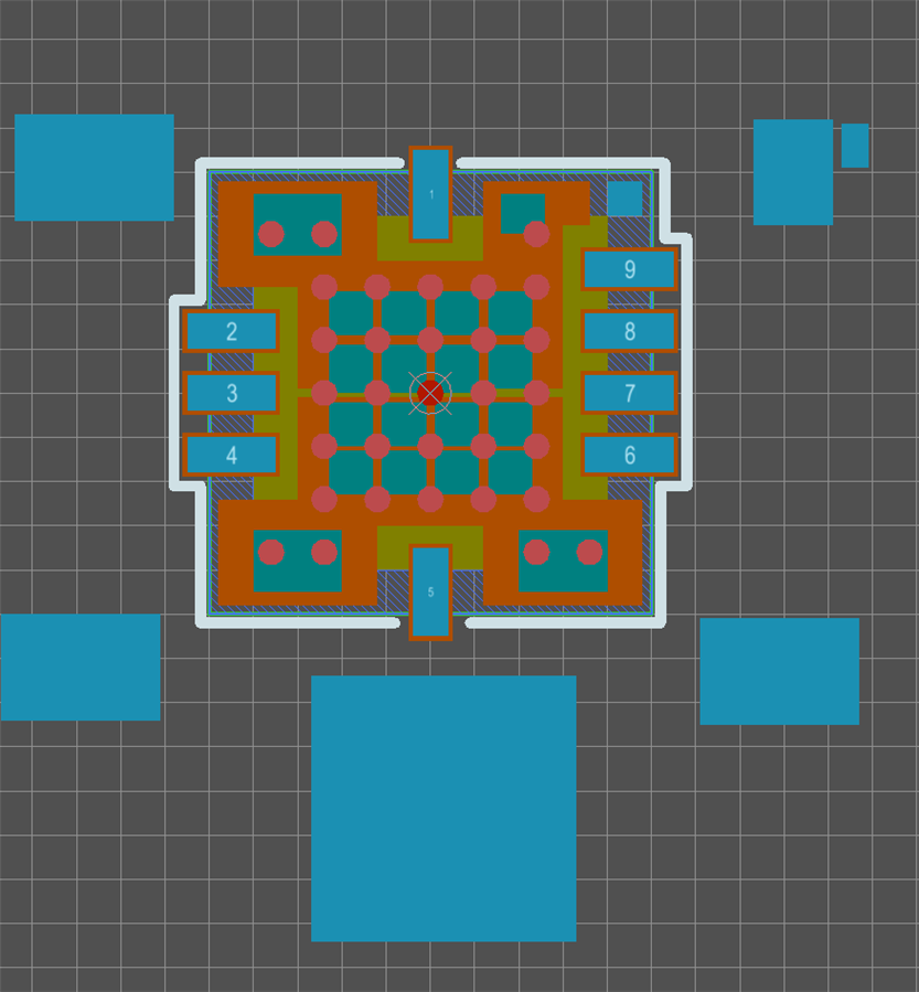
For example, I would like to make a copper ground pad for this LLGA-9 package like this:

image

In order to make that irregular ground pad shape I pieced together a number of regular rectangle shapes like these:

image

Is that how irregular fill shapes are made in CS? 

If that is the case, how do these or any final shape get assigned a net connection?  To I have to subsequently go back an edit each piece of the shape to attach a net name?

Thank you,

Stuart

  • Cancel

Top Replies

  • nhee
    nhee over 4 years ago +1 suggested
    It's similar to Orcad although probably not in the same order (as I recall). Click the Polygon Pour tool. Make your selections of name, pour style, associated net, locked, poured or not, etc. Your cursor…
  • tarribred61
    tarribred61 over 4 years ago in reply to nhee +1 suggested
    Yes, this can be done using the polygon pour. That would be done on the PCB level. To make an irregular shape on the footprint I suggest searching for "Altium Designer custom footprint" and read a number…
  • nhee
    nhee over 4 years ago in reply to tarribred61 +1 suggested
    Good points regarding an arbitraty footprint shape. #2 makes it a piece of cake. And regardless of method, it's always a good idea to examine your Gerber outputs to see if you're getting what you hoped…
Parents
  • nhee
    0 nhee over 4 years ago

    It's similar to Orcad although probably not in the same order (as I recall).


    Click the Polygon Pour tool.

    Make your selections of name, pour style, associated net, locked, poured or not, etc.

    Your cursor turns into a large vertical cross.

    Draw your polygon with as many vertices as you desire.

    When you close the polygon and escape out of the command, it will be poured with the style you chose.


    There is also a tab in the dialog box for entering actual vertex coordinates.

    This can be handy if, for instance, you were laying out a PCB antenna from a specific design or, if you were

    entering the shape from a spreadsheet with IPC rules, etc.

    • Cancel
    • Vote Up +1 Vote Down
    • Cancel
  • tarribred61
    0 tarribred61 over 4 years ago in reply to nhee

    Yes, this can be done using the polygon pour.  That would be done on the PCB level.


    To make an irregular shape on the footprint I suggest searching for "Altium Designer custom footprint" and read a number of related threads.


    Summary wise:

    1) You can combine pads by overlapping them and give them the same pad number to match the schematic symbol pin.  When a net is connected to the pin all the pads will pick up the net name.

    2) You can draw a custom shaped polygon on the copper layer and corresponding shapes on the paste and/or solder mask layers.  If these overlay with a pad then the copper will connect to the pad net.

    • Cancel
    • Vote Up +1 Vote Down
    • Cancel
  • nhee
    0 nhee over 4 years ago in reply to tarribred61

    Good points regarding an arbitraty footprint shape.  #2 makes it a piece of cake.


    And regardless of method, it's always a good idea to examine your Gerber outputs to see if you're getting what you hoped for.

    • Cancel
    • Vote Up +1 Vote Down
    • Cancel
Reply
  • nhee
    0 nhee over 4 years ago in reply to tarribred61

    Good points regarding an arbitraty footprint shape.  #2 makes it a piece of cake.


    And regardless of method, it's always a good idea to examine your Gerber outputs to see if you're getting what you hoped for.

    • Cancel
    • Vote Up +1 Vote Down
    • Cancel
Children
  • tarribred61
    0 tarribred61 over 4 years ago in reply to nhee

    There is a benefit to using #1 method.  If you combine overlapping pads then they will be subject to the mask expansion rules.  If you use arbitrary shapes then they do not change with rule changes.  For some footprints it might not matter much.  For others that are more generic, such as some four pin voltage regulator devices, then having the rules helps reuse of the footprint.


    For the LGA shapes above, the center pad shape may be using windowed paste mask anyway so paste mask expansion rule isn't so important.  I would probably draw as shapes on the various layers to get that.

    • Cancel
    • Vote Up +1 Vote Down
    • Cancel
element14 Community

element14 is the first online community specifically for engineers. Connect with your peers and get expert answers to your questions.

  • Members
  • Learn
  • Technologies
  • Challenges & Projects
  • Products
  • Store
  • About Us
  • Feedback & Support
  • FAQs
  • Terms of Use
  • Privacy Policy
  • Legal and Copyright Notices
  • Sitemap
  • Cookies

An Avnet Company © 2025 Premier Farnell Limited. All Rights Reserved.

Premier Farnell Ltd, registered in England and Wales (no 00876412), registered office: Farnell House, Forge Lane, Leeds LS12 2NE.

ICP 备案号 10220084.

Follow element14

  • X
  • Facebook
  • linkedin
  • YouTube