element14 Community
element14 Community
    Register Log In
  • Site
  • Search
  • Log In Register
  • About Us
  • Community Hub
    Community Hub
    • What's New on element14
    • Feedback and Support
    • Benefits of Membership
    • Personal Blogs
    • Members Area
    • Achievement Levels
  • Learn
    Learn
    • Ask an Expert
    • eBooks
    • element14 presents
    • Learning Center
    • Tech Spotlight
    • STEM Academy
    • Webinars, Training and Events
    • Learning Groups
  • Technologies
    Technologies
    • 3D Printing
    • FPGA
    • Industrial Automation
    • Internet of Things
    • Power & Energy
    • Sensors
    • Technology Groups
  • Challenges & Projects
    Challenges & Projects
    • Design Challenges
    • element14 presents Projects
    • Project14
    • Arduino Projects
    • Raspberry Pi Projects
    • Project Groups
  • Products
    Products
    • Arduino
    • Avnet Boards Community
    • Dev Tools
    • Manufacturers
    • Multicomp Pro
    • Product Groups
    • Raspberry Pi
    • RoadTests & Reviews
  • Store
    Store
    • Visit Your Store
    • Choose another store...
      • Europe
      •  Austria (German)
      •  Belgium (Dutch, French)
      •  Bulgaria (Bulgarian)
      •  Czech Republic (Czech)
      •  Denmark (Danish)
      •  Estonia (Estonian)
      •  Finland (Finnish)
      •  France (French)
      •  Germany (German)
      •  Hungary (Hungarian)
      •  Ireland
      •  Israel
      •  Italy (Italian)
      •  Latvia (Latvian)
      •  
      •  Lithuania (Lithuanian)
      •  Netherlands (Dutch)
      •  Norway (Norwegian)
      •  Poland (Polish)
      •  Portugal (Portuguese)
      •  Romania (Romanian)
      •  Russia (Russian)
      •  Slovakia (Slovak)
      •  Slovenia (Slovenian)
      •  Spain (Spanish)
      •  Sweden (Swedish)
      •  Switzerland(German, French)
      •  Turkey (Turkish)
      •  United Kingdom
      • Asia Pacific
      •  Australia
      •  China
      •  Hong Kong
      •  India
      •  Korea (Korean)
      •  Malaysia
      •  New Zealand
      •  Philippines
      •  Singapore
      •  Taiwan
      •  Thailand (Thai)
      • Americas
      •  Brazil (Portuguese)
      •  Canada
      •  Mexico (Spanish)
      •  United States
      Can't find the country/region you're looking for? Visit our export site or find a local distributor.
  • Translate
  • Profile
  • Settings
Altium CircuitStudio
  • Products
  • Manufacturers
  • Altium CircuitStudio
  • More
  • Cancel
Altium CircuitStudio
Altium CircuitStudio Forum Not-fitted components visible on the paste layers
  • Blog
  • Forum
  • Documents
  • Events
  • Polls
  • Members
  • Mentions
  • Sub-Groups
  • Tags
  • More
  • Cancel
  • New
Join Altium CircuitStudio to participate - click to join for free!
Actions
  • Share
  • More
  • Cancel
Forum Thread Details
  • Locked Locked
  • Replies 5 replies
  • Subscribers 86 subscribers
  • Views 1504 views
  • Users 0 members are here
  • variants
  • circuitstudio
Related
This discussion has been locked.
You can no longer post new replies to this discussion. If you have a question you can start a new discussion

Not-fitted components visible on the paste layers

obywatel_lk
obywatel_lk over 2 years ago

Hello,

The PCB company called  me and that they have an issue. I have a PCB with variant that goes to manufacture a stencil. In a variant view I don't see components in 3D view and that is OK. I see them on top paste layer. Bom is correct - no not fitted components. Pick and place files are OK.

Here is a 3D view:

image

Here is a top paste layer:

image

I have "hide not fitted components option" checked

image

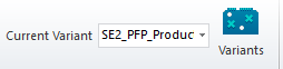
I have a variant ON:

image

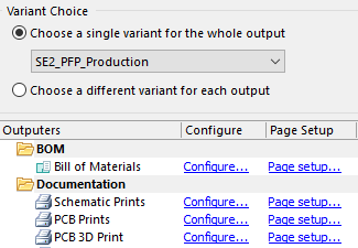
I'm generating outputs with variants:

image

I have all components matched:

image

No warnings, no errors.

Could you tell me what is wrong and if it is a CircuitStudio bug?

  • Cancel

Top Replies

  • charlieo21
    charlieo21 over 2 years ago in reply to obywatel_lk +1
    I have seen in various PCBs that there's paste in the DNP footprints, it doesn't hurt having paste in the pads and if in the future you want to populate a part the paste is already there. Removing the…
  • GabeFromSpace
    GabeFromSpace over 2 years ago

    What did the PCB company say their issue was?

    Also, if those circular pads are for probing with a multimeter, test fixture, etc. I'd recommend removing their paste. Solder paste has flux in it that can leave a hard nonconductive coating over solder joints which makes it difficult to probe.

    • Cancel
    • Vote Up 0 Vote Down
    • Cancel
  • obywatel_lk
    obywatel_lk over 2 years ago in reply to GabeFromSpace

    Hello Gabriel,

    Thanks for quick answer. They saw a paste on test points - and there should be no paste so good catch. My issue is, that the paste is on the all not fitted components (top paste / bottom paste layer), so they almost manufactured a stencil with all components (Even these not fitted) despite the variant is correctly turned on and gerber files are generated specifically for this variant.

    • Cancel
    • Vote Up 0 Vote Down
    • Cancel
  • charlieo21
    charlieo21 over 2 years ago in reply to obywatel_lk

    I have seen in various PCBs that there's paste in the DNP footprints, it doesn't hurt having paste in the pads and if in the future you want to populate a part the paste is already there. Removing the paste from the DNPs would require another stencil, having paste in all the pads only need one stencil.

    • Cancel
    • Vote Up +1 Vote Down
    • Cancel
  • GabeFromSpace
    GabeFromSpace over 2 years ago in reply to obywatel_lk

    Like Charlieo said, putting solder paste on DNP components shouldn't hurt. With my footprint library, solder paste of choice, and stencil preferences, an 0603 takes less than $0.00045 worth of solder paste. Not really something to worry about unless you have dozens of DNPs & you're making tens of thousands of boards.

    For the test points, everybody has their unique design & library preferences. But I generally make a "test point" library component to put in the schematics, then I set the "Paste Mask Expansion" on the pad in the footprint to -10mm, so it effectively gets rid of the paste layer.

    • Cancel
    • Vote Up 0 Vote Down
    • Cancel
  • obywatel_lk
    obywatel_lk over 2 years ago

    Thank you for all replies. I created a pad class for all unwanted pads and removed the paste by adding a clearance in "Past Mask Expansion Rule". The question is whether this is the intended implementation of the functionality (?)

    • Cancel
    • Vote Up 0 Vote Down
    • Cancel
element14 Community

element14 is the first online community specifically for engineers. Connect with your peers and get expert answers to your questions.

  • Members
  • Learn
  • Technologies
  • Challenges & Projects
  • Products
  • Store
  • About Us
  • Feedback & Support
  • FAQs
  • Terms of Use
  • Privacy Policy
  • Legal and Copyright Notices
  • Sitemap
  • Cookies

An Avnet Company © 2025 Premier Farnell Limited. All Rights Reserved.

Premier Farnell Ltd, registered in England and Wales (no 00876412), registered office: Farnell House, Forge Lane, Leeds LS12 2NE.

ICP 备案号 10220084.

Follow element14

  • X
  • Facebook
  • linkedin
  • YouTube