This is reproducible
Steps to reproduce:
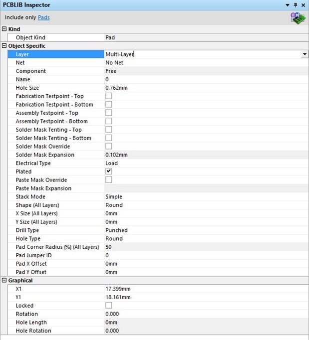
1. Add a pad to a PCB Library Component
2. Open PCBLIB Inspector
3. Select the pad (it should be a multi-layer pad by default.) Settings should be as follows:
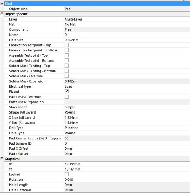
4. Click in the Layer row, and change to a single layer (e.g. Top Layer)
5. Expected result is the same as doing this in the pad editing dialog (changing to a single layer pad), the actual result is the pad is still a multi-layered pad but with zero set in the X-size and Y-size. See below.