


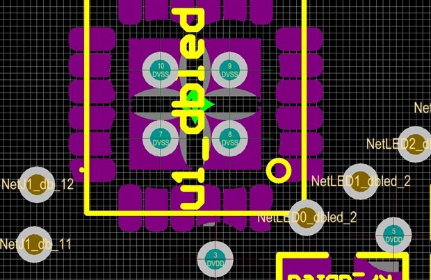
I have a weird effect. Via/pad power plane connection patterns are affecting the solder mask layer on my board. Has anyone seen this before ?

I have a weird effect. Via/pad power plane connection patterns are affecting the solder mask layer on my board. Has anyone seen this before ?
