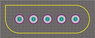
Create a footprint with pins named "1","2" and "3" etc
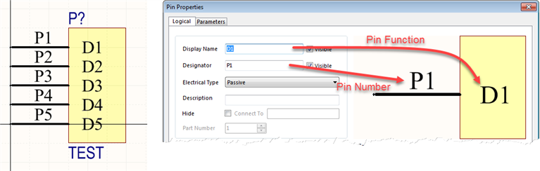
Then create a schematic symbol with pins names "P1", "P2", "P3" etc
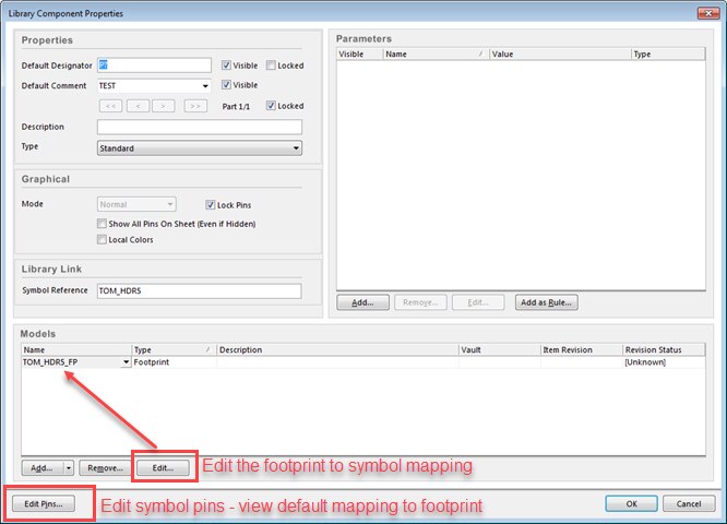
Link the footprint model to the schematic symbol. Click on the Edit Pins button in the Library Component Properties dialogue box.
The pin names for the footprint are incorrectly labelled "P1", "P2", and "P3" etc
If you assume CircuitStudio has correctly mapped the pins, you are wrong. When you go to import the part into a PCB design document via ECO you will get error messages saying that there is no corresponding pin in the selected footprint.