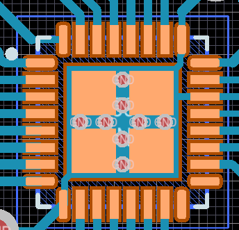
I'm trying to create a custom pad shape in the PCB footprint library editor. I want the pad to be a "T" shape.
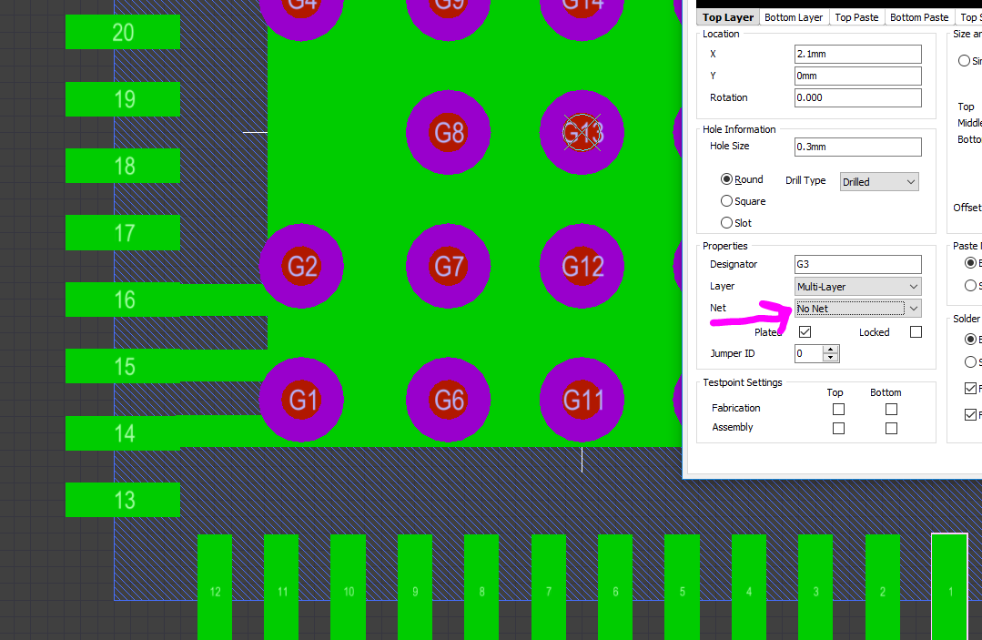
I have created a solid region of the shape I desire. How do I specify the solder and paste mask expansion values for this shape?
How do I designate this shape as being a "pad", so that I can associate schematic symbol pins to it?