element14 Community
element14 Community
    Register Log In
  • Site
  • Search
  • Log In Register
  • Community Hub
    Community Hub
    • What's New on element14
    • Feedback and Support
    • Benefits of Membership
    • Personal Blogs
    • Members Area
    • Achievement Levels
  • Learn
    Learn
    • Ask an Expert
    • eBooks
    • element14 presents
    • Learning Center
    • Tech Spotlight
    • STEM Academy
    • Webinars, Training and Events
    • Learning Groups
  • Technologies
    Technologies
    • 3D Printing
    • FPGA
    • Industrial Automation
    • Internet of Things
    • Power & Energy
    • Sensors
    • Technology Groups
  • Challenges & Projects
    Challenges & Projects
    • Design Challenges
    • element14 presents Projects
    • Project14
    • Arduino Projects
    • Raspberry Pi Projects
    • Project Groups
  • Products
    Products
    • Arduino
    • Avnet Boards Community
    • Dev Tools
    • Manufacturers
    • Multicomp Pro
    • Product Groups
    • Raspberry Pi
    • RoadTests & Reviews
  • About Us
  • Store
    Store
    • Visit Your Store
    • Choose another store...
      • Europe
      •  Austria (German)
      •  Belgium (Dutch, French)
      •  Bulgaria (Bulgarian)
      •  Czech Republic (Czech)
      •  Denmark (Danish)
      •  Estonia (Estonian)
      •  Finland (Finnish)
      •  France (French)
      •  Germany (German)
      •  Hungary (Hungarian)
      •  Ireland
      •  Israel
      •  Italy (Italian)
      •  Latvia (Latvian)
      •  
      •  Lithuania (Lithuanian)
      •  Netherlands (Dutch)
      •  Norway (Norwegian)
      •  Poland (Polish)
      •  Portugal (Portuguese)
      •  Romania (Romanian)
      •  Russia (Russian)
      •  Slovakia (Slovak)
      •  Slovenia (Slovenian)
      •  Spain (Spanish)
      •  Sweden (Swedish)
      •  Switzerland(German, French)
      •  Turkey (Turkish)
      •  United Kingdom
      • Asia Pacific
      •  Australia
      •  China
      •  Hong Kong
      •  India
      •  Korea (Korean)
      •  Malaysia
      •  New Zealand
      •  Philippines
      •  Singapore
      •  Taiwan
      •  Thailand (Thai)
      • Americas
      •  Brazil (Portuguese)
      •  Canada
      •  Mexico (Spanish)
      •  United States
      Can't find the country/region you're looking for? Visit our export site or find a local distributor.
  • Translate
  • Profile
  • Settings
Altium CircuitStudio
  • Products
  • Manufacturers
  • Altium CircuitStudio
  • More
  • Cancel
Altium CircuitStudio
Documents Gerber - Failed to Match All Shapes
  • Blog
  • Forum
  • Documents
  • Events
  • Polls
  • Members
  • Mentions
  • Sub-Groups
  • Tags
  • More
  • Cancel
  • New
Join Altium CircuitStudio to participate - click to join for free!
Actions
  • Share
  • More
  • Cancel
Engagement
  • Author Author: e14softwareuk
  • Date Created: 13 Feb 2018 10:28 AM Date Created
  • Last Updated Last Updated: 6 Oct 2021 9:30 PM
  • Views 1450 views
  • Likes 0 likes
  • Comments 0 comments
Related
Recommended

Gerber - Failed to Match All Shapes

This is a rarely encountered error that can occur when generating your Gerber outputs (extended RS274X format).

image

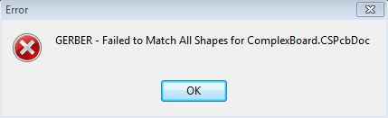
It is nothing to panic about, the cause is known and workarounds are available.


The Gerber format uses Apertures (D-Codes) for drawing your circuit. You can think of Apertures as different pen sizes, typically each unique shape and track width will have an Aperture assigned and the plot image is made up of 'flashed' and 'drawn' apertures to create the plot. CircuitStudio supports a maximum aperture number (D-Code) of 999 so if you have too many unique shapes in your design it will trigger this error. Complex shapes link polygons do not need their own aperture but fills (Home | Fill) do when using the extended format (RS274X).


We cover three potential solutions that will allow you to generate your Gerber output and get your board manufactured.


1. Output Layers Individually

Typically a single layer will not require more than the maximum number of apertures so you can use Outputs | Gerber and generate one layer at a time. Depending on your design it may be possible to select several layers, you will need to experiment. Use RS274X format and all the information regarding the Aperture assignments are contained within the Gerber file itself so it is safe to generate the files individually.


2. Don't Use Embedded Apertures (RS274X)

CircuitStudio supports the older Gerber format where the Aperture definitions are placed into a separate file and each plot layer then makes use of those common definitions. It is recommended to generate all layers at once with this format to prevent any mismatch between the definitions and the drawn layers. When using this option ensure that Gerber Setup : Apertures : Flash all fills it not checked to prevent an excessive number of apertures being required.

image

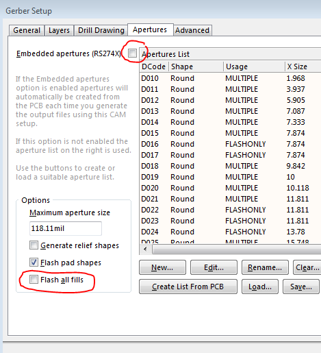
After selecting the layers to plot (this should be all the layers required), Clear the list and then click Create List From PCB to calculate the required apertures. Scroll down the list to make sure you have not reached D999, if you have then too many apertures are required and you should consider using a different workaround technique.


3. Switch from using Fills to Polygons

You can determine if the number of fills used on a design is likely to be a problem. Click View | Filter then in the PCB Filter window select Groups:<All>, Objects:Fill and Layers:<All>. At the bottom of the window you will get a count of objects that pass the filter. If this is a high number (approaching 900 or more) then it is very likely that the number of fills is causing your Gerber output error. If you want to use extended Gerber format then you can either use the first workaround (generating one layer at a time) or rework your design to use polygons rather than rectangular fills.

  • pcb
  • cam
  • circuitstudio
  • Share
  • History
  • More
  • Cancel
  • Sign in to reply
element14 Community

element14 is the first online community specifically for engineers. Connect with your peers and get expert answers to your questions.

  • Members
  • Learn
  • Technologies
  • Challenges & Projects
  • Products
  • Store
  • About Us
  • Feedback & Support
  • FAQs
  • Terms of Use
  • Privacy Policy
  • Legal and Copyright Notices
  • Sitemap
  • Cookies

An Avnet Company © 2025 Premier Farnell Limited. All Rights Reserved.

Premier Farnell Ltd, registered in England and Wales (no 00876412), registered office: Farnell House, Forge Lane, Leeds LS12 2NE.

ICP 备案号 10220084.

Follow element14

  • X
  • Facebook
  • linkedin
  • YouTube