

If it often a requirement to include one or more logos on a PCB, this may be a company logo or regulatory mark. There are a few different ways to accomplish this and it may be a little bit of trial and error to see what works best for your particular design. Once a logo has been imported or designed you can save as a library component to allow easy re-use. This document covers the following methods:
- Design With CircuitStudio
- Bitmap Import
- DXF Import
- Custom TrueType Font
1. Design With CircuitStudio
For simple designs the tools available within CS can be sufficient to create a graphic.You have a good range of tools including lines, arcs, circles, text, fills, regions and polygons.
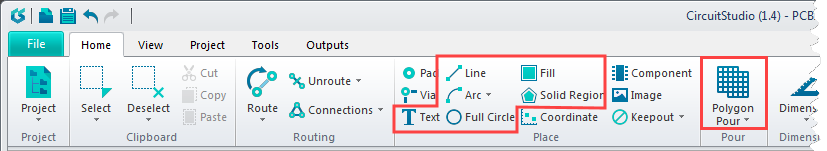
A little explanation of the difference may help.
Home | Fill - a filled polygonal shape with any number of vertices
Home | Solid Region - a simple filled rectangular shape
Home | Polygon Pour - a filled polygonal shape that will repour around other objects
Some useful tips to help control the drawing process, these apply to both drawing shapes and routing tracks so well worth knowing if you are not familiar. Whilst in the drawing process where the cursor has changed and you are placing vertices you can change the elbow direction and the placement mode (angle constraints and straight lines/arcs). Hit F1 (or SHIFT+F1) when drawing to see the available shortcuts.
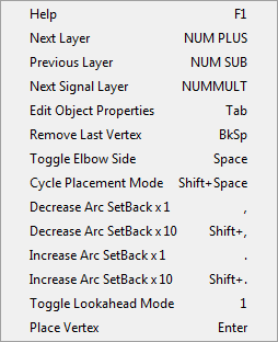
The most common shortcuts are described below.
SPACE (Toggle Elbow Side) - Changes the initial starting direction of the line segment, for example toggling between a horizontal or vertical start.
SHIFT+SPACE (Cycle Placement Mode) - Toggles though the various placement modes which are Line 45/90; Line 90/45; Line 90/45 with Arc; Line 90/90; Line 90/90 with Arc.
BACKSPACE - Undo the last vertex placed
, or . or SHIFT+, or SHIFT+. - Adjust arc radius (small increments, larger increments with SHIFT)
2. Bitmap Import
CS includes the ability to import a bitmap graphic using Home | Image. The supported graphic formats are BMP, PNG, JPG and GIF.
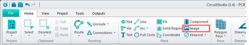
Although you can import colour and greyscale images remember that they are always converted to just black and white (or more accurately filled and transparent pixels) to fit with being drawn on a single PCB layer. You will need to resize your image prior to import, once imported you cannot resize each pixel is fixed at 8mil (0.2mm) square. This pixel size can be an issue for some designs, especially if needing very fine detail to be reproduced which leads to the import looking a little 'blocky'. Technically it is possible to manually resize/reshape the image because it consists of region objects and bringing up the property dialog for a region allows the vertices to be edited although this is not normally a practical method.
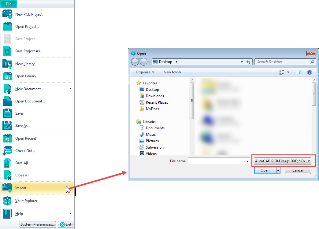
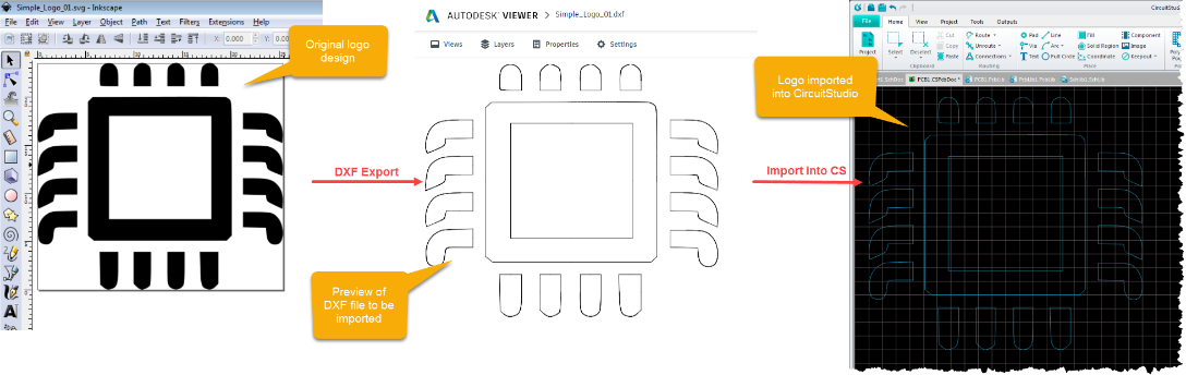
3. DXF Import
DXF is a very common format to use for importing logos, typically only an outline will be imported and any solid fills from the original design lost due to the file format, only outlines will remain.
Here's a simple example of a logo drawn using a graphics package, exported to DXF and then imported to CS. As we can see the DXF version has lost the fills so we will aim to restore within CS.
Fill using Regions
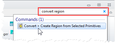
There are a couple of techniques that can be used to fill the logo. For simple objects you can often select an outline and convert to a filled region. To access the required command you first need to select the outline that is to be filled and then type "convert region" into the search box and click on the command.
If successful a solid region will be created. If the outline was non-contiguous or a composed of a set of complex line segments (as can often happen with DXF exports) this command can fail and no region will be created. All is not lost though, we will move on to using a polygon pour to fill the logo.
Fill using Polygon Pours
To have polygon pours work make sure all logo objects (DXF import and polygons) are placed on a copper layer (e.g. Top layer). Once the work is complete the logo can be moved to a different layer.
Draw a polygon pour using Home | Polygon Pour over the entire outline logo. Because the polygon will not be connected to a new it is important to untick Remove Dead Copper otherwise the whole polygon will self-delete as it has no electrical connection. We give the polygon a name so that we can identify it easily.
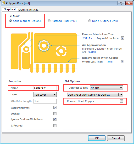
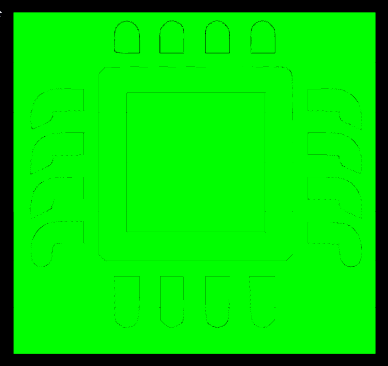
Once poured we get something like the image below. Note that if your imported DXF consisted of thousands of segments then polygon pouring (in particular bringing up the properties dialog afterwards) can be slow.
The default clearance rules are affecting the pour causing a large gap to be left between the outline and the pour. To correct this we just need to configure the design rules using the following process.
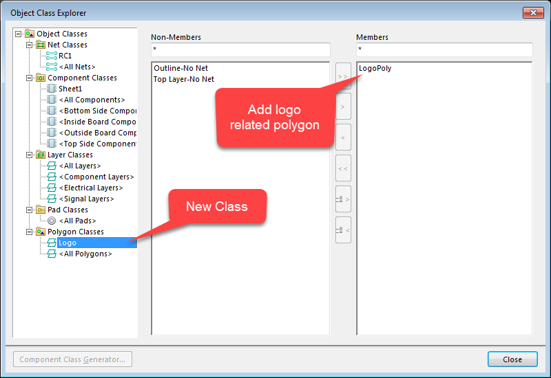
- Bring up the classes dialogue using Home | Classes.
- In the Object Class Explorer dialog select Polygon Classes, right click and Add Class. Right click on the new class and select Rename Class, change to Logo (or whatever you prefer).
- With Logo class selected move your polygon (named LogoPoly) across from Non-Members to Members.
- Close the Object Class Explorer dialog.
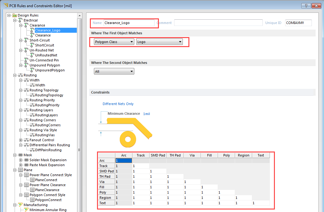
Next define the design rules that will adjust the clearance around the logo polygon.
- Bring up the rules editor with Home | Design Rules.
- Define a new Electrical > Clearance rule (highlight rule type then click New Rule button)
- Edit the rule properties - change name to Clearance_Logo, match against Polygon Class = Logo, all constraints to 0 or 1 (using 1 lets you see the original DXF outline easily).
- Click OK the accept the new values then close the dialog.
- Select the logo polygon, right click and execute Polygon Actions > Rebuild Selected
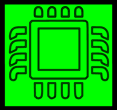
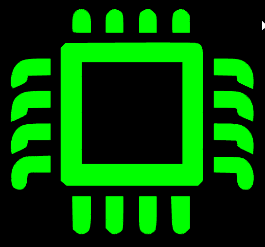
Once done we have a polygon that very closely matches the DXF outline. Next we turn it into a fixed object (so it doesn't repour) and delete parts to just leave behind the fills we need.
- Select logo polygon, right click Polygon Actions > Explode Selected Polygons To Free Primitives.
- Left click on areas that are not to be filled and delete them.
That's it, you now have a logo. If necessary you can use View | Object Inspector to change the logo onto the desired layer (e.g. Top Overlay).
4. Custom TrueType Font
A completely different approach that can overcome the limitations of DXF where too many drawing objects are created when importing for CS to easily work with. The exact details of this method will depend on the software you have access to and the format of the logo.
- Create a SVG logo file
- e.g. Use Inkscape* or Adobe Illustrator* to draw a logo and save as SVG.
- e.g. Use QCAD* to import an existing DXF logo and export as SVG.
- Convert SVG to a TTF font file
- e.g. icomoon.io can be used to create the font file
- Assign the new glyph to an easy to access key (.e.g. 'a')
- Install your custom font file in Windows
- Right click and select Install to make the font available to Windows programs.
- This font will need to be available on any computer you use with CS.
- Your manufacturing partner will not need the font file if you are supplying Gerbers.
- Open the PCB document in CS and place text using your custom font
- Add text, type in the character associated with your logo (.e.g 'a').
- Change text properties to use TrueType font and select your custom logo font.
- Adjust the logo size as you would for any text string.
*These are examples only, we are not recommending this software/service or suggesting that it is fit for purpose.
Top Comments
-

shabaz
-
Cancel
-
Vote Up
+1
Vote Down
-
-
Sign in to reply
-
More
-
Cancel
Comment-

shabaz
-
Cancel
-
Vote Up
+1
Vote Down
-
-
Sign in to reply
-
More
-
Cancel
Children