element14 Community
element14 Community
    Register Log In
  • Site
  • Search
  • Log In Register
  • Community Hub
    Community Hub
    • What's New on element14
    • Feedback and Support
    • Benefits of Membership
    • Personal Blogs
    • Members Area
    • Achievement Levels
  • Learn
    Learn
    • Ask an Expert
    • eBooks
    • element14 presents
    • Learning Center
    • Tech Spotlight
    • STEM Academy
    • Webinars, Training and Events
    • Learning Groups
  • Technologies
    Technologies
    • 3D Printing
    • FPGA
    • Industrial Automation
    • Internet of Things
    • Power & Energy
    • Sensors
    • Technology Groups
  • Challenges & Projects
    Challenges & Projects
    • Design Challenges
    • element14 presents Projects
    • Project14
    • Arduino Projects
    • Raspberry Pi Projects
    • Project Groups
  • Products
    Products
    • Arduino
    • Avnet Boards Community
    • Dev Tools
    • Manufacturers
    • Multicomp Pro
    • Product Groups
    • Raspberry Pi
    • RoadTests & Reviews
  • About Us
  • Store
    Store
    • Visit Your Store
    • Choose another store...
      • Europe
      •  Austria (German)
      •  Belgium (Dutch, French)
      •  Bulgaria (Bulgarian)
      •  Czech Republic (Czech)
      •  Denmark (Danish)
      •  Estonia (Estonian)
      •  Finland (Finnish)
      •  France (French)
      •  Germany (German)
      •  Hungary (Hungarian)
      •  Ireland
      •  Israel
      •  Italy (Italian)
      •  Latvia (Latvian)
      •  
      •  Lithuania (Lithuanian)
      •  Netherlands (Dutch)
      •  Norway (Norwegian)
      •  Poland (Polish)
      •  Portugal (Portuguese)
      •  Romania (Romanian)
      •  Russia (Russian)
      •  Slovakia (Slovak)
      •  Slovenia (Slovenian)
      •  Spain (Spanish)
      •  Sweden (Swedish)
      •  Switzerland(German, French)
      •  Turkey (Turkish)
      •  United Kingdom
      • Asia Pacific
      •  Australia
      •  China
      •  Hong Kong
      •  India
      •  Korea (Korean)
      •  Malaysia
      •  New Zealand
      •  Philippines
      •  Singapore
      •  Taiwan
      •  Thailand (Thai)
      • Americas
      •  Brazil (Portuguese)
      •  Canada
      •  Mexico (Spanish)
      •  United States
      Can't find the country/region you're looking for? Visit our export site or find a local distributor.
  • Translate
  • Profile
  • Settings
Altium CircuitStudio
  • Products
  • Manufacturers
  • Altium CircuitStudio
  • More
  • Cancel
Altium CircuitStudio
Documents Controlling Net Connection visibility
  • Blog
  • Forum
  • Documents
  • Events
  • Polls
  • Members
  • Mentions
  • Sub-Groups
  • Tags
  • More
  • Cancel
  • New
Join Altium CircuitStudio to participate - click to join for free!
Actions
  • Share
  • More
  • Cancel
Engagement
  • Author Author: e14softwareuk
  • Date Created: 9 May 2019 10:59 AM Date Created
  • Last Updated Last Updated: 9 May 2019 1:47 PM
  • Views 1852 views
  • Likes 0 likes
  • Comments 0 comments
Related
Recommended

Controlling Net Connection visibility

Net connections are the "air wires" that indicate the connectivity of the PCB using thin lines drawn between unrouted points on the board. There are several methods to control the visibility of these connections as outlined below.


Show/Hide Net Connections UI

The user interface provides options to show and hide net connections right down to the individual net level. Launch the viewing panel from View | PCB > Nets.

image

The nets panel lists your net classes at the top, nets that are members of the selected class next and finally the primitive objects that make up the nets. A quick way to toggle visibility is to click <All Nets>, right click > Connections > Show or Hide. In addition the Show/Hide option is also available on individual nets.

image

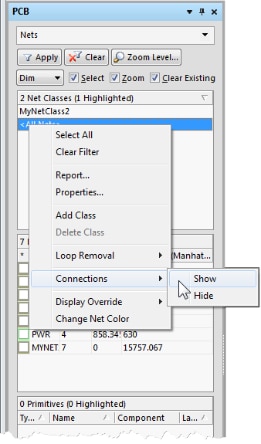
The Change Net Color option in the above menu allows selecting a different colour for the display of net connections and can be applied to individual nets.


View Configurations

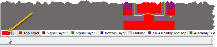
The View Configurations dialog can be used to control the visibility of net connections allowing for a global on/off and the default colour. This dialog can be invoked by clicking the coloured box next to LS in the lower left of the PCB editor window.

image

image


Single Layer Mode

Single layer mode is configurable to show just the selected layer (tab set at bottom of PCB editor window), grey out other layers or monochrome other layers. Less known is the option to change how net connections are shown.


From the View Configurations dialog select View Options tab you can control if all nets should be shown or just those that have a connection to the current layer.

image

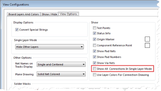
Another option that may be of interest is the one below - Use Layer Colors For Connection Drawing.


'Hidden' Command

Using the search box (top right) allows control of net connections by component.

image

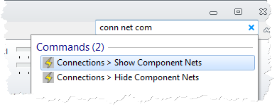
This mode activates a selection cursor allowing components to be clicked on to turn on/off their connection lines.


If Connections Are Not Showing Correctly

Try Tools | Netlist > Clean All Nets. This has been known to sort out designs where only some net connections were displayed.

  • pcb
  • circuitstudio
  • Share
  • History
  • More
  • Cancel
  • Sign in to reply
element14 Community

element14 is the first online community specifically for engineers. Connect with your peers and get expert answers to your questions.

  • Members
  • Learn
  • Technologies
  • Challenges & Projects
  • Products
  • Store
  • About Us
  • Feedback & Support
  • FAQs
  • Terms of Use
  • Privacy Policy
  • Legal and Copyright Notices
  • Sitemap
  • Cookies

An Avnet Company © 2025 Premier Farnell Limited. All Rights Reserved.

Premier Farnell Ltd, registered in England and Wales (no 00876412), registered office: Farnell House, Forge Lane, Leeds LS12 2NE.

ICP 备案号 10220084.

Follow element14

  • X
  • Facebook
  • linkedin
  • YouTube