This and other great measurement tips and tricks can be found on the General Purpose Electronics Test Equipment Blog
Monday, March 26, 2012
Fine Tuning the FPGA Power-on Process
Powering on an FPGA can be careful balancing act of proper sequencing and slew rate timing on multiple power supply inputs. Some of the reasons for this balancing act is to ensure the power-on-reset circuit is not tripped, to ensure proper operation of the PLL, and to minimize in-rush current which is especially important in low power applications. In this post we will look at how modern multiple output power supplies can be used for fine tuning the FPGA turn-on process with an emphasis on minimizing in-rush current.
Modern multiple output power supplies have three features that make them a valuable tool for tuning the FPGA turn-on process, they are:
- Adjustable output sequencing feature that allows the users to setup the turn-on time for each of the power supply's outputs.
- Slew rate adjustment to specify the rise time at turn-on for each power supply output.
- Output current and voltage digitizers for capturing the in-rush current, spotting voltage sags, etc.
The modern multiple output power supply comes into the FPGA circuit design process before implementing the power distribution system for the circuit. Use the modern multiple output power supply to tune the sequencing turn-on timing and slew rate to find the ideal turn-on conditions for the FPGA circuit. While tuning the turn on timing, the power supply measurement digitizers are used to measure the resulting voltage and the resulting in-rush current at turn-on. After the tuning process, the power distribution system can be designed and setup to achieve the ideal sequence and slew rate timing established earlier with the modern multiple output power supply.
Let's look at a quick example using a low power FPGA circuit that is going into a portable battery powered device. The engineer designing the power distribution system for the FPGA circuit wants to keep power usage to a minimum, which includes tuning the power turn-on conditions such that in-rush current is kept to a minimum amount while ensuring proper turn-on of the circuit. To tune the power turn-on conditions the engineer is using Keysight's N6705B DC Power Analyzer as the modern multiple output power supply. The N6705B is a modular power supply that supports up to 4 outputs. The N6705B has output sequencing, slew rate control, and output measurement digitizers along with a scope like display to analyze the digitized measurements.
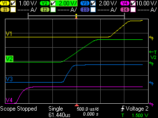
The FPGA circuit under test has four supply inputs. The engineer sets each of the N6705B outputs according to the specified ranges of the FPGA. A test run was done to verify the sequencing and slew rate of the power supply outputs. The result was captured on the N6705B's display and it can be seen in the below figure.
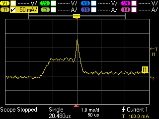
V1, V2, and V3 were all used for powering the FPGA. V4 was used for other components in the circuit. V1 is the FPGA's core supply and that is where we want to measure the in-rush current. Using the timing parameters shown in the above figure, the in-rush current on the core supply was captured and is shown in the figure below.
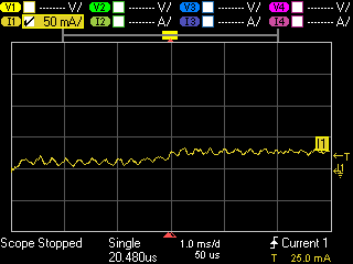
As you can see in the figure the in-rush current consists of two spikes. The first is just over 1 ms with a flat top and the second is a higher current shorter duration spike. After the in-rush current, the low power FPGA's standby static current settles to about 15 mA. The engineer then did a number of tuning iterations of the same test. At each iteration the sequencing or the slew rate time was adjusted with the goal of minimizing the in-rush current. After tuning the engineer was able to get the in-rush current down to essentially zero (see figure below) while still maintaining a proper turn-on of the circuit.
In this post we looked at how a modern power supply with features such as output sequencing, slew rate control, and measurement digitizers can be used to tune the power input turn-on characteristics of an FPGA or any other embedded circuit for designing the power distribution. This is valuable when trying to ensure proper turn-on every time and to minimize in-rush current for power optimization. Below is a link to get more information on Keysight's N6705B DC Power Analyzer and also a link to a good TI app note that discusses properly powering on an FPGA. If you have any questions just email me and if you have any comments use the "Comments" section below.
Click here for more information on the N6705B DC Power Analyzer
TI app note "Tips for successful power-up of today’s high-performance FPGAs"


