


As our ability to shrink the size of transistors begins approaching the atomic wall, researchers have had to shift more of their focus on making chips more efficient in both power consumption, and the speed at which the chips can process data. One way to do this is to simplify the design of the chip to utilize fewer components, but that’s easier said than done. Researchers at Purdue University have recently published a research paper that could change the way we build microchips forever.
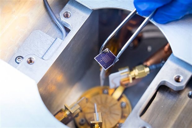
Researchers have created a more feasible way to combine transistors and memory on a chip, potentially bringing faster computing. (Caption Credit: Purdue University | Photo/Vincent Walter)
The paper which was published in Nature Electronics in December of 2019 details a new transistor/memory hybrid that has the potential to temporarily alleviate some of the issues that chipmakers are facing right now. The team of engineers had to find a way to combine ferroelectric RAM with silicon-based transistors, a problem that has frustrated researchers for decades.
You see, silicon and materials with high ferroelectric properties do not like to mix for a number of reasons, and previous attempts to make the two materials play nice together were for all intended purposes, fruitless. The closest we have been able to get (until now) to this holy grail of combinations is interfacing the ferroelectric RAM as a separate module on the chip itself.
The team was led by Peide Ye, Professor of Electrical and Computer Engineering at Purdue, together they discovered ho
“We used a semiconductor that has ferroelectric properties. This way two materials become one material, and you don’t have to worry about the interface issues,” said Peide Ye, Professor of Electrical and Computer Engineering at Purdue and team lead of this project.
The new hybrid was dubbed a “ferroelectric semiconductor field-effect transistor and is built using the same process as traditional silicon-based chips. “The material, alpha indium selenide, not only has ferroelectric properties but also addresses the issue of a conventional ferroelectric material usually acting as an insulator rather than a semiconductor due to a so-called wide “band gap,” which means that electricity cannot pass through and no computing happens,” the researchers wrote. “Alpha indium selenide has a much smaller band gap, making it possible for the material to be a semiconductor without losing ferroelectric properties.”
The transistor was built and tested by Mengwei Si, a postdoctoral researcher at Purdue, and the results showed that it was on-par in terms of performance of traditional silicon transistors. Performance is expected to increase substantially with improvements in efficiency and refinement as further research and testing is conducted. Furthermore, both teams worked together in conjunction with the Georgia Institute of Technology to build alpha indium selenide into a space on a chip, called a ferroelectric tunneling junction, which engineers could use to enhance a chip’s capabilities even further.
This has been an issue with other ferroelectric materials in the past as their band gap made the material much too thick for any usable electrical current to pass through. Alpha indium selenide has a much smaller band gap, and can retain its properties at a thickness of just 10-nanometers, which allows much more current to flow through a smaller space which results in further miniaturization of integrated circuits. The paper says that this new technology could allow scales down to just several nanometers to become the norm for microchip fabrication in the near future. This technology could one day shrink circuit density to a scale that allows us to memic networks similar to how the human brain transfers information.
I covered the computer processor beat for several years early in my career, and I remember when 16nm scale processes were thought to be close to the atomic wall, but each year or two we somehow managed to shrink things down further, and then over the last decade or so, that progress has slowed to what can only be described as a glacier's pace. I have been pretty bummed out about this, but its research like this that gives me hope that we can squeeze more performance out of silicon-based processors yet!