


The Precise Demands of Semiconductor Manufacturing
As predicted by Moore’s Law, the semiconductor manufacturing process continues to advance at a rapid pace with each subsequent generation of technology reducing the size and spacing of features and layers on the integrated circuits (ICs). This greater density of circuitry on a wafer requires both greater precision and a more delicate fabrication process.
Many of the newer, more complex ICs today consist of a dozen or more layers produced in 300+ sequenced processing steps. Then, once the wafers are complete there is post-processing followed by IC packaging and testing. Here is a summary of the some of the typical steps in the IC manufacturing process:
- Wafer processing
- Cleaning of the silicon wafers
- Surface passivation
- Photolithography
- Etching
- Various depositions (chemical, atomic, physical)
- Wafer testing
- Die preparation
- Wafer mounting
- Wafer backgrinding and polishing
- Wafer bonding and stacking
- Wafer bumping (if needed for flip chips)
- Through-silicon via (TSV) manufacture (if needed for 3D ICs)
- Die cutting
- IC packaging
- Die attachment to a substrate
- IC bonding (such as wire bonding)
- IC encapsulation
- Laser marking and silkscreen printing
- IC testing
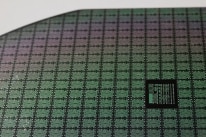
Figure 1 – Image of Silicon Wafer with Etched Circuitry
Today, semiconductor manufacturing places very high demands on pressure measurement technology to ensure a high-quality process. All steps in fabrication, including cleaning, etching, and polishing, need to be extremely precise as the uniformity of the finished products are measured in microns. Thus, throughout all aspects of semiconductor manufacturing, testing and inspection are performed to measure variances.
The Role of Pressure Sensors in Semiconductor Manufacturing
Pressure sensors are used throughout IC manufacturing to perform real-time pressure measurements during the various stages of the semiconductor process. Some the common uses include:
- Improving the precision and control of the wafer polishing heads through consistent application of pressure. In chemical mechanical polishing (CMP) systems, measurements such as characterization and parallelism of the polishing heads is an important part of the fabrication process.
- Ensuring consistent wafer cleaning by confirming the effectiveness of the wafer polishing head. If the polishing head is not properly conditioned, or it lacks a consistent roughness on its surface, then external particles will not be properly removed. Any particle residue can result in ICs that fail inspection and test.
- Reducing the amount of cracked or unbounded wafers. As mentioned, CMP is a crucial manufacturing process for semiconductors as improving uniformity during the polishing process is key. An uneven polishing head can lead to cracks in the wafer, resulting in ICs being thrown away.
- Verify die-to-substrate planarization, especially for flip-chip bonding. Uniform pressure is required to avoid die cracking or open electrical connections. Just like wafer cracking, an IC with an open electrical connection or a damaged die inside cannot be used.
- Identifying wear on plates and other parts that could result in wafer bonding errors. In order to apply level amounts of pressure during attachment, the plates need to be even. However, over time they and other components are subject to wear that can cause them to become uneven. By identifying the pressure variations, the equipment can signal the problem and generate a repair alarm before faulty parts are assembled.
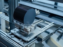
Figure 2 – Image of Wafers in Fabrication
Superior Sensor’s NimbleSenseTM Architecture for Semiconductor Manufacturing
Having an extremely low noise floor, the NimbleSense architecture is ideal for the precise pressure measurements required by semiconductor equipment to improve long-term stability, maximize accuracy and increase overall IC production yields. However, the NimbleSense advantages extend beyond the low noise floor. Some of its application-specific building blocks provide additional value add for semiconductor manufacturing.
Multi-Range TechnologyTM
Multi-Range technology allows one pressure sensor to operate at maximum performance over several different pressure ranges. As wafer lots have different numbers of layers, and bonding/packaging can vary, the pressure requirements will differ. Multi-Range allows one sensor to be adjusted without any performance degradation to meet the pressure requirements for different fabrication processes.
Advanced Digital Filtering
Semiconductor manufacturing requires precision, and any external factors such as noise from air conditioning or other equipment, building vibrations, etc. can impact the accuracy of pressure sensors. Utilizing our integrated advanced digital filtering technology, Superior’s pressure sensors eliminate the noise created by these factors prior to their reaching the sensor sub-system. Thus, the noise is eliminated before it becomes an error signal that can lead to inaccurate readings.
Conclusion
Semiconductor manufacturing continues to advance at a rapid pace with each subsequent generation of technology reducing the size and spacing of features and layers on ICs. This greater density of circuitry on a wafer places very high demands on pressure measurement technology to ensure a high-quality process. All steps in fabrication need to be extremely precise as the uniformity of the finished products are measured in microns.
Superior Sensor’s unique pressure sensor technology, based on our proprietary NimbleSense architecture, provides many benefits for semiconductor equipment including excellent long-term stability, higher accuracy, advanced digital filtering and Multi-Range technology. To learn more about the NimbleSense architecture, please visit our technology page. If you have a semiconductor-related project you would like to discuss, please contact us.