


PCB Design
PCB design is one of the most important steps in the development of a project and must be done well and checked many times in order to avoid the finished product flat out not working due to some electrical error on the PCB In this project we were limited to using a double sided board which was more than enough layers to accommodate the switching regulator backup linear regulator jumper pins and all the peripherals mentioned in previous blog posts including the Nokia 5110 LCD display Joystick buttons and piezo-electric buzzer Another constraint is that the PCB cannot be more than 80mm x 100mm which is comparable to the size of the FRDM-K64FFRDM-K64F microcontroller itself since this PCB is going to have header pins that allot it to slot into the GPIO of the K64F Also since the game I will be creating is made for a mobile hand-held design a PP3 9V battery is being used to power it since this battery is quite bulky it will be mounted underneath the micro-controller with a battery lead connecting it to the PCB The general procedure for PCB design is as follows
- Create Schematic
- Get parts from bill of meterials
- Do electrical rule check (ERC)
- Lay down parts in board view
- Route tracks
- Add power polygons
- Do design rule check (DRC)
Schematic Design
The first steps in designing a PCB is to complete the PCB schematic which makes placement and routing of the physical PCB a lot easier later on. Each peripheral is connected in its own small module like group with nets that connect each outside connection to another small module. This allows us to easily visualize each building block of the system which will help in component placement later on because on the PCB board, components from the same module are often physically grouped together for ease of routing. The schematic diagram is a quick and easy step but makes life in the board view a lot easier especially because it generates a ratsnest which is a visualisation of how all the components are connected to each other. The finished schematic diagram is attached below.
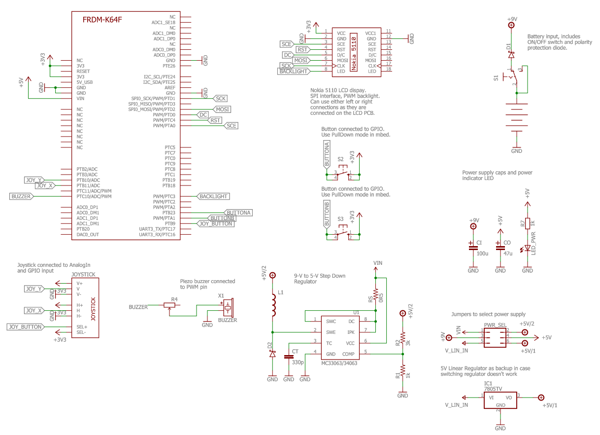
The electrical rule check (ERC) is used to make sure that you haven't made a mistake when connecting up each component which it checks using assumed parameters about your circuits. For example when the ERC check was performed it returned several errors linking to the LED and other components not having values. Some of these errors can be ignored because in this case we do not care what value an LED has (assumed 'value' means parameters like resistance), instead we care about how it is connected to the other components in the circuit. Another few errors encountered were to do with the LCD display not having some of its pins connected up but from prior knowledge we know that the pins on one side of the LCD screen are identical to the pins on the other side so only one side is really required to be connected, in our case the GND from both sides were connected because these will be taken care of when drawing polygons in the board view.
Board View
After completing the schematic diagram and checking its electrical connections using both the ERC and going over it manually we can start assembling the components on the board view. In EAGLE, which is the PCB CAD I am using to design the PCB, we can convert straight from the schematic view to the borad view where there will be a web of yellow connecting lines between components called a ratsnest. These connections really help to organise the location of each component in relation to its connections to everything else and the first step of the board design is to place everything in suitable locations. If enough time is not spent on component placement then routing the tracks between components is going to become a lot harder later on and will require much more complicated traces including PTH (plated through holes also known as vias) to get from one component connection to another. The mark of a good PCB designer is not a complicated PCB but a complicated circuit with a very simply routed PCB. In my design I had to re-think through my component placement several times to get it just right, especially when other factors come in to play such as the switching regulator circuit needing to be very compact in order to reduce noise and interference between it and any other lines.
Originally I had the switching regulator components mounted on the back of the PCB to hide the circuitry but was then advised to place them on the front so that soldering would be easier so instead I placed them on the front of the PCB but behind the LCD display. I was only able to do this because the display is going to be mounted on header pins slightly above the PCB so there is some space underneath where the screen would be that I can place relatively low profile components. Obviously the power switch, battery leads and other components that the user is going to want to access cannot be hidden behind the screen so these were placed around the edge of the PCB for easier accessibility. I placed the joystick on the left hand side of the screen and the A and B buttons on the right hand side of the screen to get the old game-boy feeling except with a joystick instead of a D-pad. Another alteration I made for the sake of routing the PCB traces more efficiently and neatly was that I swapped which pins the buttons connected to on the microcontroller so that their traces would run parallel instead of crossing. The finished PCB design is shown below:
You may notice that the ground connections of everything are not connected up using traces and you would be correct. Instead, polygons are used that fill the remaining copper of the PCB with ground planes on both the front and back of the board because this allows the ground connections to have less resistance which is always a good thing. On the diagram above the ground planes are represented by the dotted lines surrounding the PCB and are not filled in in this diagram to make seeing the traces on the front and back easier. There was also a constraint where no solder pads were allowed to be placed above the ethernet port of the microcontroller seen here by the grey rectangle next to the LCD because they might touch and short out which is not desirable.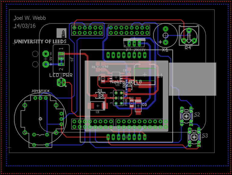
After designing the layout of the PCB as you want it the next step is to 'smash' the components to separate their labels so you can delete their values as required and to write the name and date. Also it is important to check for any airwires that you might have forgotten to create traces for, an easy but unorthodox way of doing this in EAGLE is to zoom out as far as possible so the PCB looks like a small square, then click using the wiring tool on the small square and if any airwires exist then it will pick them up and you can zoom back in to see where it is meant to be connected. Finally the design rule check (DRC) must be completed that checks your design against a plethora of different parameters, the important ones in our case were a minimum track and gap of 0.08inches or 8mil and a minimum polygon isolation of 8mil. Once the DRC check is completed and there are no errors then do the checks again just to be on the safe side because as mentioned previously this is possibly the most crucial stage in designing a product and one small mistake would cause the entire product not to work. Once completed and checked many times then it is ready to submit to a board house for manufacture!
Top Comments