element14 Community
element14 Community
    Register Log In
  • Site
  • Search
  • Log In Register
  • Community Hub
    Community Hub
    • What's New on element14
    • Feedback and Support
    • Benefits of Membership
    • Personal Blogs
    • Members Area
    • Achievement Levels
  • Learn
    Learn
    • Ask an Expert
    • eBooks
    • element14 presents
    • Learning Center
    • Tech Spotlight
    • STEM Academy
    • Webinars, Training and Events
    • Learning Groups
  • Technologies
    Technologies
    • 3D Printing
    • FPGA
    • Industrial Automation
    • Internet of Things
    • Power & Energy
    • Sensors
    • Technology Groups
  • Challenges & Projects
    Challenges & Projects
    • Design Challenges
    • element14 presents Projects
    • Project14
    • Arduino Projects
    • Raspberry Pi Projects
    • Project Groups
  • Products
    Products
    • Arduino
    • Avnet & Tria Boards Community
    • Dev Tools
    • Manufacturers
    • Multicomp Pro
    • Product Groups
    • Raspberry Pi
    • RoadTests & Reviews
  • About Us
  • Store
    Store
    • Visit Your Store
    • Choose another store...
      • Europe
      •  Austria (German)
      •  Belgium (Dutch, French)
      •  Bulgaria (Bulgarian)
      •  Czech Republic (Czech)
      •  Denmark (Danish)
      •  Estonia (Estonian)
      •  Finland (Finnish)
      •  France (French)
      •  Germany (German)
      •  Hungary (Hungarian)
      •  Ireland
      •  Israel
      •  Italy (Italian)
      •  Latvia (Latvian)
      •  
      •  Lithuania (Lithuanian)
      •  Netherlands (Dutch)
      •  Norway (Norwegian)
      •  Poland (Polish)
      •  Portugal (Portuguese)
      •  Romania (Romanian)
      •  Russia (Russian)
      •  Slovakia (Slovak)
      •  Slovenia (Slovenian)
      •  Spain (Spanish)
      •  Sweden (Swedish)
      •  Switzerland(German, French)
      •  Turkey (Turkish)
      •  United Kingdom
      • Asia Pacific
      •  Australia
      •  China
      •  Hong Kong
      •  India
      •  Korea (Korean)
      •  Malaysia
      •  New Zealand
      •  Philippines
      •  Singapore
      •  Taiwan
      •  Thailand (Thai)
      • Americas
      •  Brazil (Portuguese)
      •  Canada
      •  Mexico (Spanish)
      •  United States
      Can't find the country/region you're looking for? Visit our export site or find a local distributor.
  • Translate
  • Profile
  • Settings
PCB Design, Prototyping and Production
  • Products
  • More
PCB Design, Prototyping and Production
PCB Blogs Ground Paths - Useful explanation for anyone who is confused.
  • Blog
  • Forum
  • Documents
  • Leaderboard
  • Files
  • Members
  • Mentions
  • Sub-Groups
  • Tags
  • More
  • Cancel
  • New
Join PCB Design, Prototyping and Production to participate - click to join for free!
  • Share
  • More
  • Cancel
Group Actions
  • Group RSS
  • More
  • Cancel
Engagement
  • Author Author: Andrew J
  • Date Created: 15 Jan 2021 3:39 PM Date Created
  • Views 1252 views
  • Likes 11 likes
  • Comments 51 comments
Related
Recommended

Ground Paths - Useful explanation for anyone who is confused.

Andrew J
Andrew J
15 Jan 2021

EDIT 31/1/21: I've added a reply below with an embedded video which is worth watching after reading the white paper.


I've been reading around about grounding for PCBs over the last couple of days and opinions seem to fall into either "Star grounding, all the way" or "Ground plane, all the way".  Everyone has an opinion and a seemingly limitless  number of solutions based on one of those two approaches.  Any white paper that attempts to explain Star Ground seems to immediately drop down into mixed-signal grounding with the star ground as the point analog and digital grounds are joined.  Generally, any explanation seems incomplete and assumptive on the reader's level of knowledge and understanding - often in respect to esoteric points to do with dialectrics, expansion beyond traces, equations and so on.  It's all pretty confusing for the most part.


However, I did come across this white paper from Maxim Integrated "Successful PCB Grounding with Mixed-Signal Chips - Follow the Path of Least Impedance" which seems to be the best explanation I've found of how DC, low frequency and high frequency currents flow in respect to ground and does so in a way that is understandable and not just in mixed signal chips, despite it's title.  Actually, it's a lot about mixed-signal chips but it does so with a clear explanation of the DC and AC components of any current and thus offers a degree of clarity I've not found elsewhere for any sort of circuit/IC.  It also describes approaches to laying out parts on a PCB in a way that is clear.  In many respects, it covers the topic similarly to others, but in a way that hasn't made assumptions on understanding of the reader.


It does approach the topic by using a ground plane and that left me wondering how a star ground approach would work.   For DC current, it's seems clear: it would follow the trace back to the source which would be the power source; for AC I'm less clear.  I've copied an image from the paper below and then reproduced it with my own representation using a Star Ground approach (actually, two approaches):


image

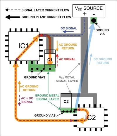
Maxim paper image showing current flow on a ground plane between two ICs


image

My representation of Maxim's image but using a Star Ground, where the star point is the ground pin of the power source


image

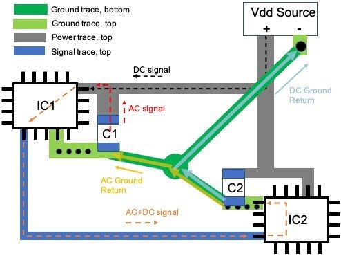
My alternate representation using a Star Ground where the star point is centralised then returned to the power source.


Obviously, the example given to explain how currents flow is pretty simple and in reality will be more complex because there will be many signals flowing across traces and power planes.  Could I start a discussion on some points to help me fill in some blanks:

  1. Have I got my representation of AC return flow in a Star Ground right?
  2. Would one of my two representations be better than the other - I'm inclined to think the second one purely from the more direct route for AC return but that is a longer path for DC
  3. This just shows one signal but obviously there would be other returns, eg DC from IC1 that would flow to VDD source; AC from the Vdd Source that is bypassed by C1 and C2 and returns to Vdd source etc.  In the case of star ground that is 'against' the flow of what I show for the AC return current flow but even on a ground plane there must be some contention.  Is that what causes heat and noise in the trace/plane?  Is that a misunderstanding I have?
  • Sign in to reply
  • Andrew J
    Andrew J over 4 years ago in reply to fmilburn

    Some of it, like habit 3, will come down to a tradeoff I guess. With 2 layer boards coming in manufactured at < $1.50 for anything up to 100mm x 100mm then if you can be flexible on size you can be - I see OshPark charge by the square inch though.


    Habit 7a is an interesting one as well.  I have 3 ICs at the moment all of which the datasheet calls for a 10uF tantalum and a 100nF mlcc.  I rather suspect that this could be swapped for a reasonable size mlcc, e.g. 10uF or 22uF but because the datasheet says do X I don't have the empirical experience to take the risk!!  The main point though is body size as opposed to capacitance size: there will be a minimum capacitance needed but you can add more.  The key is small size to keep the induction loop down - I don't think I could hand solder much below 0805 and I tried 0602 but not very well.  If ESR is needed by the IC (e.g. a LDO output) then bigger body size caps (electrolytics say) might be needed to get that, but the datasheet should say.  This, again, is where reality bites: how many ICs have a datasheet that says put the decoupling caps as close as possible to the power pins but they build the chip where these pins are on opposite sides and corners!!


    If you do a search on YouTube for Eric Bogatin you'll find a couple of videos where he explains some of this in a bit more detail, particularly 7b.  There's a video demonstrating that: if you do fill and tie it properly then it has a small positive impact (on his demo, it improved crosstalk by about 0.2% over not doing it); getting it wrong has pretty drastic results though so I wouldn't do it as I have no idea how to tie the fills together in the right way.  I think both Eric and Rick gave a figure of 3xtrace width separation to get crosstalk down to <5%.


    The thing is, I don't know how much of this is applicable at high frequency and how much at low frequency so for most of what I do it may be irrelevant.  An interesting understanding point I got though, is that frequency is related to signal rise times so if you can slow them down and still have a working circuit that's a good thing to do.  As ICs get smaller then the rise times get faster: the new Raspberry Pi Pico probably has really fast rise times.

    • Cancel
    • Vote Up 0 Vote Down
    • Sign in to reply
    • More
    • Cancel
  • fmilburn
    fmilburn over 4 years ago in reply to Andrew J

    Hi Andrew,


    That is a really good link!  It has the kind of cook book stuff (with all the caveats) that are practical and easy to apply.

    • Habit 1:  Use small traces and vias. I had no idea about the trace widths but it does make sense when I think about it.  I have generally been making larger traces thinking that was a good thing to do, or at least did no harm.
    • Habit 2: Keep components, signals, and power paths on layer 1 and ground return by way of a ground plane on layer 2. I'm pretty good about that.
    • Habit 3: Adjust components for less congestion and maximize signal separation.  Sometimes I am trying to make a PCB as small as possible.  I can improve on separating signals when possible for sure though.
    • Habit 4: Minimize cross-under on the bottom layer and make them short, use return straps for long cross unders.  To be honest I had never heard of return straps but will remember that one.
    • Habit 5:  Use the largest size capacitor in the smallest body... usually 22 uF MLCC for decoupling capacitors. It always seemed to me it should be best to use larger ones but I usually use what is on the datasheet which often has a lower value.  Might as well use one larger size exclusively.
    • Habit 6:  Allocate one return for each digital signal when possible on connectors. I often do this but it wasn't something I thought about.
    • Habit 7a: Don't use different value capacitors (e.g. 10 uF, 1 uF, and 0.1 uF for each power pin).  I don't know that I have seen 3 different values recommended, but datasheets often shown 2 different values.  Sometimes the larger one is a tantalum. I wonder how that guideline originated and why. 
    • Habit 7b: Never use a copper fill.  I definitely haven't followed that one.  Pretty sure I've made less than ideal copper fills as well.  I understand better now why it isn't particularly useful: "If there is room to add a copper fill between signal traces, the spacing between traces will be large enough to probably have acceptably low cross talk". 


    Italics on "probably"  are mine :-).  It is enough to make me stop doing ground copper fills on the top layer though.  Thanks, I have bookmarked this one.

    • Cancel
    • Vote Up 0 Vote Down
    • Sign in to reply
    • More
    • Cancel
  • Andrew J
    Andrew J over 4 years ago in reply to fmilburn

    Hey Frank fmilburn,


    Check this out: https://www.signalintegrityjournal.com/blogs/12-fundamentals/post/1207-seven-habits-of-successful-2-layer-board-designers.  Some eye-opening points there, particularly about trace widths.

    • Cancel
    • Vote Up 0 Vote Down
    • Sign in to reply
    • More
    • Cancel
  • Andrew J
    Andrew J over 4 years ago in reply to fmilburn

    You’re asking me? imageimage  I’d say yes to most of those points but would query the ground pour on top.

    I Always find the “keep the ground plane as intact as possible” alongside ‘plenty of stitching vias between top and bottom” rather contrary and I have no idea what the right response would be.  I would say though that I’ve seen enough recently from Rick Hartley and Eric Bogatin saying NOT to bother flood filling because it adds very little IF you get it right but can be really bad if you get it wrong (and guess what it’s easy to do!)  Of course there are plenty of people with different views so I suppose the key is “who do you know and trust”.


    It would seem that the potential for crosstalk through coupling is something to be aware of, both with trace routing and nearby flood fills so the spacing is important so not routing alongside seems like a good idea unless you want the coupling (e.g. for the forward and return traces)


    I Can’t even work out if “copper balancing” is important or just another thing that is parroted because they read it somewhere.  That then needs flood fills and stitching vias and broken up ground planes and close fills. It’s a roundabout image  And how many stitching vias so as not to break up the ground plane?

    It’s nearly as cheap to get a 4-layer board made as a 2-layer, particularly if you can keep dimensions max 100mm x 100mm.

    • Cancel
    • Vote Up 0 Vote Down
    • Sign in to reply
    • More
    • Cancel
  • fmilburn
    fmilburn over 4 years ago in reply to Andrew J

    If I start doing 4 layer boards I probably will.  Meanwhile for a 2 layer board:


    • realize all designs have high frequency components
    • separate analog and digital
    • keep the ground plane on the back layer as clean as possible
    • minimize the number of tracks jumped and do it at 90 degrees
    • do a ground pour on the top layer
    • place plenty of vias between top and bottom ground pours and at both ends of isolated pours
    • don't connect the Faraday cage / chassis to the circuit ground


    What did I leave out for a 2 layer board? image

    • Cancel
    • Vote Up 0 Vote Down
    • Sign in to reply
    • More
    • Cancel
>
element14 Community

element14 is the first online community specifically for engineers. Connect with your peers and get expert answers to your questions.

  • Members
  • Learn
  • Technologies
  • Challenges & Projects
  • Products
  • Store
  • About Us
  • Feedback & Support
  • FAQs
  • Terms of Use
  • Privacy Policy
  • Legal and Copyright Notices
  • Sitemap
  • Cookies

An Avnet Company © 2025 Premier Farnell Limited. All Rights Reserved.

Premier Farnell Ltd, registered in England and Wales (no 00876412), registered office: Farnell House, Forge Lane, Leeds LS12 2NE.

ICP 备案号 10220084.

Follow element14

  • X
  • Facebook
  • linkedin
  • YouTube