element14 Community
element14 Community
    Register Log In
  • Site
  • Search
  • Log In Register
  • Community Hub
    Community Hub
    • What's New on element14
    • Feedback and Support
    • Benefits of Membership
    • Personal Blogs
    • Members Area
    • Achievement Levels
  • Learn
    Learn
    • Ask an Expert
    • eBooks
    • element14 presents
    • Learning Center
    • Tech Spotlight
    • STEM Academy
    • Webinars, Training and Events
    • Learning Groups
  • Technologies
    Technologies
    • 3D Printing
    • FPGA
    • Industrial Automation
    • Internet of Things
    • Power & Energy
    • Sensors
    • Technology Groups
  • Challenges & Projects
    Challenges & Projects
    • Design Challenges
    • element14 presents Projects
    • Project14
    • Arduino Projects
    • Raspberry Pi Projects
    • Project Groups
  • Products
    Products
    • Arduino
    • Avnet Boards Community
    • Dev Tools
    • Manufacturers
    • Multicomp Pro
    • Product Groups
    • Raspberry Pi
    • RoadTests & Reviews
  • Store
    Store
    • Visit Your Store
    • Choose another store...
      • Europe
      •  Austria (German)
      •  Belgium (Dutch, French)
      •  Bulgaria (Bulgarian)
      •  Czech Republic (Czech)
      •  Denmark (Danish)
      •  Estonia (Estonian)
      •  Finland (Finnish)
      •  France (French)
      •  Germany (German)
      •  Hungary (Hungarian)
      •  Ireland
      •  Israel
      •  Italy (Italian)
      •  Latvia (Latvian)
      •  
      •  Lithuania (Lithuanian)
      •  Netherlands (Dutch)
      •  Norway (Norwegian)
      •  Poland (Polish)
      •  Portugal (Portuguese)
      •  Romania (Romanian)
      •  Russia (Russian)
      •  Slovakia (Slovak)
      •  Slovenia (Slovenian)
      •  Spain (Spanish)
      •  Sweden (Swedish)
      •  Switzerland(German, French)
      •  Turkey (Turkish)
      •  United Kingdom
      • Asia Pacific
      •  Australia
      •  China
      •  Hong Kong
      •  India
      •  Korea (Korean)
      •  Malaysia
      •  New Zealand
      •  Philippines
      •  Singapore
      •  Taiwan
      •  Thailand (Thai)
      • Americas
      •  Brazil (Portuguese)
      •  Canada
      •  Mexico (Spanish)
      •  United States
      Can't find the country/region you're looking for? Visit our export site or find a local distributor.
  • Translate
  • Profile
  • Settings
PCB Design, Prototyping and Production
  • Products
  • More
PCB Design, Prototyping and Production
PCB Blogs KiCAD 8: create symbol for Rohm complementary MOSFET pair US6M2
  • Blog
  • Forum
  • Documents
  • Leaderboard
  • Files
  • Members
  • Mentions
  • Sub-Groups
  • Tags
  • More
  • Cancel
  • New
Join PCB Design, Prototyping and Production to participate - click to join for free!
  • Share
  • More
  • Cancel
Group Actions
  • Group RSS
  • More
  • Cancel
Engagement
  • Author Author: Jan Cumps
  • Date Created: 14 Sep 2024 7:17 PM Date Created
  • Views 2431 views
  • Likes 6 likes
  • Comments 16 comments
  • mosfet
  • kicad
  • US6M2
  • rohm
  • symbol editor
Related
Recommended

KiCAD 8: create symbol for Rohm complementary MOSFET pair US6M2

Jan Cumps
Jan Cumps
14 Sep 2024

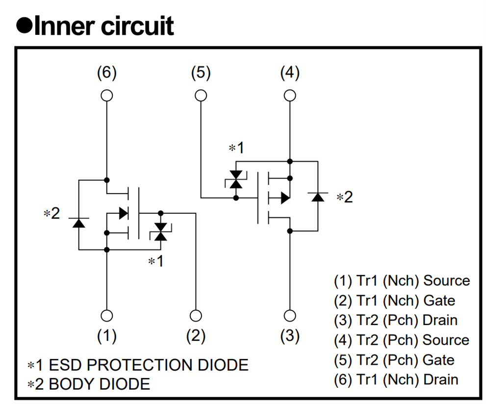
Rohm's US6M2 is an IC with 2 complementary MOSFETs on a single chip. With gate-source protection diodes.
I'm using them in a design, but KiCAD doesn't have a symbol for this IC. It has a number of complementary MOSFET symbols (I counted 14, most of them derived from two Infineon devices). None with input protection though.

image
source: datasheet

I could have started with one of the existing ones, and add the protection diode. I chose another option.

I found a symbol for Rohm US6K4TR. This is also a component with two MOSFETS, in the same package as the US6M2. But 2 N-channel transistors instead of a complementary set. I imported that symbol in KiCAD and started a US6M2 design from that.

Initially, I used the exact same symbol, and just turned one of the two N-channel FETs into a P-channel one. I just had to 180° turn the two triangles:

image

On the image above, you see the result. On right FET I flipped the triangles of the source arrow and the body diode.

I could call it a day, job done. But the symbol is not very schematic-friendly. The component is often used as push-pull pair, or as one half of a H-bridge. And those designs are never drawn like this symbol. 

Luckily, KiCAD has the option to split a single component into several symbols. That's what I used here. One symbol for the N-channel FET, and one for the P-channel.

image

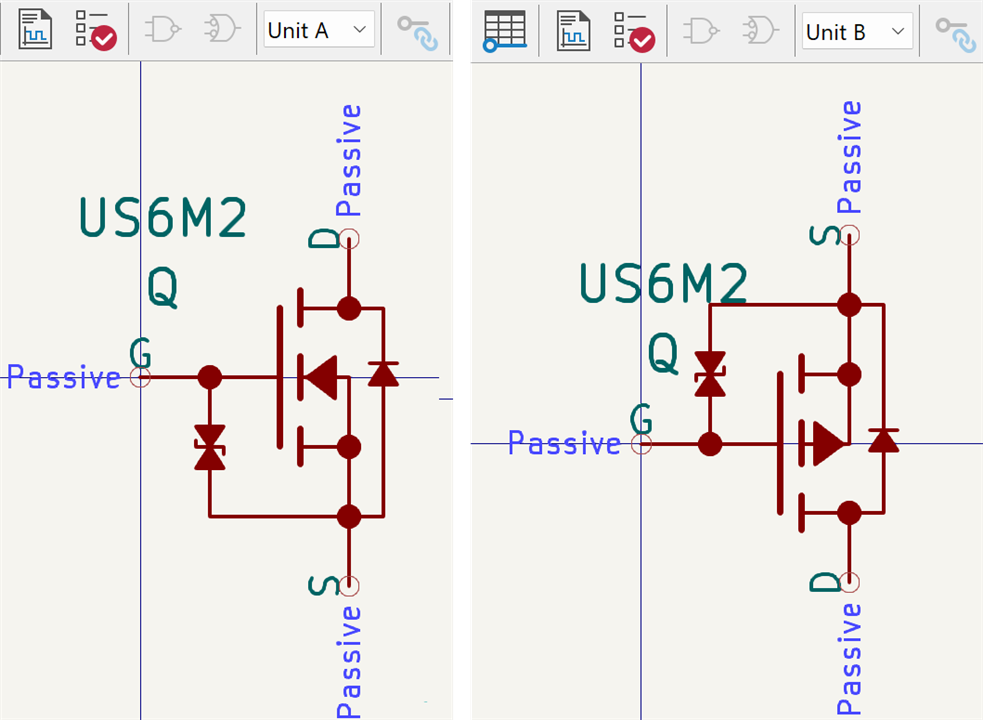
They are the same symbols as the ones I initially used. I only reorganised the pins a bit, and created the 2 separate units.

You can now add this component to your schematic. KiCAD will first prompt to place Unit A, then Unit B. When you assign component numbers to your schematic, these two will get the same number, with an A and B suffix.

Here's a schematic example. A MOSFET H-bridge, with two US6M2:

image

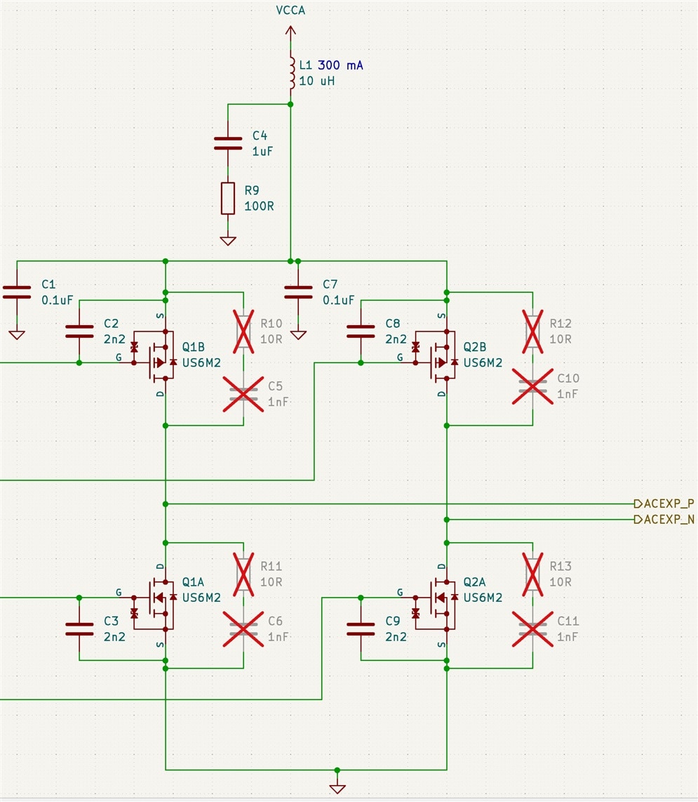
Q1 A&B are one US6M2. Q2 A&B a second one.

Would you prefer the initial symbol with both FETs combined, or the second version where there is a symbol for each of the FETs?

The symbol is available on GitHub.

  • Sign in to reply

Top Comments

  • shabaz
    shabaz 9 months ago in reply to shabaz +1
    (can't edit). Turns out there is a far simpler way! See here: https://forum.kicad.info/t/making-oval-and-half-oval-shapes-for-symbols/54078/4
  • Jan Cumps
    Jan Cumps 9 months ago in reply to jc2048

    I spotted it too :)

    • Cancel
    • Vote Up 0 Vote Down
    • Sign in to reply
    • More
    • Cancel
  • jc2048
    jc2048 9 months ago in reply to Jan Cumps

    "*or bought it."

    If so, they should ask for their money back. That's the symbol for a depletion-mode MOSFET.

    • Cancel
    • Vote Up 0 Vote Down
    • Sign in to reply
    • More
    • Cancel
  • Jan Cumps
    Jan Cumps 9 months ago

    It's common for P-channel MOSFETs to have different characteristics than their N-channel counterpart. Here, where the two are sitting in one package, it's easy to compare:

    image

    • Cancel
    • Vote Up 0 Vote Down
    • Sign in to reply
    • More
    • Cancel
  • Jan Cumps
    Jan Cumps 9 months ago in reply to Jan Cumps

    cant' edit. composite MOSFET must be complementary MOSFET

    • Cancel
    • Vote Up 0 Vote Down
    • Sign in to reply
    • More
    • Cancel
  • Jan Cumps
    Jan Cumps 9 months ago in reply to jc2048

    "Showing the ESD protection on the gate is new to me - for me that's just clutter. It's not good practice to use it as an active part of the operation of a circuit, so why does it need to be on the schematic?"

    My first idea was to use one of KiCAD's generic composite MOSFET symbols, without the protection. But then I thought: "you select these FETs specifically/only for this functionality", and that it make sense calling that out on a schematic.

    Renesas uses the US6M2, and have made their own symbol*. It includes the gate-source protection diode. That flipped me to add it to my drawing.

    image

    *or bought it. It is definitely different than the one supplied by Rohm.

    Another approach could have been to use the KiCAD generic ones, and annotate the schematic or BOM with text, showing that Q1 - Q2 should be types with input protection.

    • Cancel
    • Vote Up 0 Vote Down
    • Sign in to reply
    • More
    • Cancel
>
element14 Community

element14 is the first online community specifically for engineers. Connect with your peers and get expert answers to your questions.

  • Members
  • Learn
  • Technologies
  • Challenges & Projects
  • Products
  • Store
  • About Us
  • Feedback & Support
  • FAQs
  • Terms of Use
  • Privacy Policy
  • Legal and Copyright Notices
  • Sitemap
  • Cookies

An Avnet Company © 2025 Premier Farnell Limited. All Rights Reserved.

Premier Farnell Ltd, registered in England and Wales (no 00876412), registered office: Farnell House, Forge Lane, Leeds LS12 2NE.

ICP 备案号 10220084.

Follow element14

  • X
  • Facebook
  • linkedin
  • YouTube