element14 Community
element14 Community
    Register Log In
  • Site
  • Search
  • Log In Register
  • Community Hub
    Community Hub
    • What's New on element14
    • Feedback and Support
    • Benefits of Membership
    • Personal Blogs
    • Members Area
    • Achievement Levels
  • Learn
    Learn
    • Ask an Expert
    • eBooks
    • element14 presents
    • Learning Center
    • Tech Spotlight
    • STEM Academy
    • Webinars, Training and Events
    • Learning Groups
  • Technologies
    Technologies
    • 3D Printing
    • FPGA
    • Industrial Automation
    • Internet of Things
    • Power & Energy
    • Sensors
    • Technology Groups
  • Challenges & Projects
    Challenges & Projects
    • Design Challenges
    • element14 presents Projects
    • Project14
    • Arduino Projects
    • Raspberry Pi Projects
    • Project Groups
  • Products
    Products
    • Arduino
    • Avnet Boards Community
    • Dev Tools
    • Manufacturers
    • Multicomp Pro
    • Product Groups
    • Raspberry Pi
    • RoadTests & Reviews
  • Store
    Store
    • Visit Your Store
    • Choose another store...
      • Europe
      •  Austria (German)
      •  Belgium (Dutch, French)
      •  Bulgaria (Bulgarian)
      •  Czech Republic (Czech)
      •  Denmark (Danish)
      •  Estonia (Estonian)
      •  Finland (Finnish)
      •  France (French)
      •  Germany (German)
      •  Hungary (Hungarian)
      •  Ireland
      •  Israel
      •  Italy (Italian)
      •  Latvia (Latvian)
      •  
      •  Lithuania (Lithuanian)
      •  Netherlands (Dutch)
      •  Norway (Norwegian)
      •  Poland (Polish)
      •  Portugal (Portuguese)
      •  Romania (Romanian)
      •  Russia (Russian)
      •  Slovakia (Slovak)
      •  Slovenia (Slovenian)
      •  Spain (Spanish)
      •  Sweden (Swedish)
      •  Switzerland(German, French)
      •  Turkey (Turkish)
      •  United Kingdom
      • Asia Pacific
      •  Australia
      •  China
      •  Hong Kong
      •  India
      •  Korea (Korean)
      •  Malaysia
      •  New Zealand
      •  Philippines
      •  Singapore
      •  Taiwan
      •  Thailand (Thai)
      • Americas
      •  Brazil (Portuguese)
      •  Canada
      •  Mexico (Spanish)
      •  United States
      Can't find the country/region you're looking for? Visit our export site or find a local distributor.
  • Translate
  • Profile
  • Settings
PCB Design, Prototyping and Production
  • Products
  • More
PCB Design, Prototyping and Production
PCB Blogs KiCAD 8: RX23E-B kit - clock, debug and reset schematic
  • Blog
  • Forum
  • Documents
  • Leaderboard
  • Files
  • Members
  • Mentions
  • Sub-Groups
  • Tags
  • More
  • Cancel
  • New
Join PCB Design, Prototyping and Production to participate - click to join for free!
  • Share
  • More
  • Cancel
Group Actions
  • Group RSS
  • More
  • Cancel
Engagement
  • Author Author: Jan Cumps
  • Date Created: 28 Oct 2024 7:36 PM Date Created
  • Views 852 views
  • Likes 5 likes
  • Comments 6 comments
  • kicad
  • rx23E-B
  • renesas
Related
Recommended

KiCAD 8: RX23E-B kit - clock, debug and reset schematic

Jan Cumps
Jan Cumps
28 Oct 2024

I'm building a PCB for Renesas' RX23E-B microcontroller. In this post, I experiment with breaking the microcontroller schematic symbol into functional units. And I created some custom symbols and footprints.

image

Schematics

I'm interested to hear what you think about the schematic approach and layout choices. Some things I did for this schematic:

  • I first created a full (100 pin) symbol for the microcontroller. And for this design, split it in several functional units, to fit the schematics layout. U1E in this schematic is the unit that contains clock, reset and debug pins.
  • I created a custom schematic symbol for the TE Connectivity FSM1LPS switch.
  • I tried to arrange and group the overall schematic to feel natural
  • I attempted to limit the number of functions covered in this schematic page. The "utilitarian" functions clock, debug and reset.
  • The RX23E-A symbol I created supports alternative pin function . The schematic shows the function that's default (and sometimes the hard choice) for my design.

Footprints

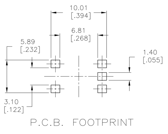
For the switch and subclock oscillator , I created a custom PCB footprint.

Switch FSM1LPS (footprint)- corrected. See misaz comment below

image  image

Crystal SSP-T7-FL:SSP-T7-FL (footprint)

image image

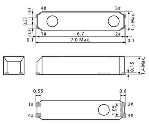
I will probably have to refine them once I created the PCB. But the pads are where they should be. Would you draw these differently?

  • Sign in to reply
  • Jan Cumps
    Jan Cumps 8 months ago

    Comparison: this is Renesas' style of schematic drawing. My design is heavily borrowing from this. But not from the style.

    image

    • Cancel
    • Vote Up 0 Vote Down
    • Sign in to reply
    • More
    • Cancel
  • Jan Cumps
    Jan Cumps 8 months ago in reply to Jan Cumps

    for history: this was my wrong pad layout:

    image

    • Cancel
    • Vote Up 0 Vote Down
    • Sign in to reply
    • More
    • Cancel
  • Jan Cumps
    Jan Cumps 8 months ago

    I tried to address both comments

    image

    Pins renumbered as caught by misaz .

    michaelkellett , related to the yellow lines (silkscreen):
    I created some more space for the pads - haven't measured yet, but will check for the clearance with the pads.
    For the line width: I adapted this part from one of the stock-KiCAD footprints. Almost all parts use that same width...

    • Cancel
    • Vote Up 0 Vote Down
    • Sign in to reply
    • More
    • Cancel
  • Jan Cumps
    Jan Cumps 8 months ago in reply to misaz

    no. Thank you - you saved me from a respin Slight smile

    • Cancel
    • Vote Up 0 Vote Down
    • Sign in to reply
    • More
    • Cancel
  • michaelkellett
    michaelkellett 8 months ago

    I like parts separated into functional blocks, although it often means re-drawing blocks according to the requirements of each new design.

    I can't be sure, but the yellow component outline looks much too thin and much too close to the copper pads.

    Most pcb houses struggle with silk screen features less than 0.15 mm line width and pad to silk screen gaps of less than 0.15 or 0.2mm.

    But it may not be correctly scaled on the footprint pictures.

    MK

    • Cancel
    • Vote Up 0 Vote Down
    • Sign in to reply
    • More
    • Cancel
>
element14 Community

element14 is the first online community specifically for engineers. Connect with your peers and get expert answers to your questions.

  • Members
  • Learn
  • Technologies
  • Challenges & Projects
  • Products
  • Store
  • About Us
  • Feedback & Support
  • FAQs
  • Terms of Use
  • Privacy Policy
  • Legal and Copyright Notices
  • Sitemap
  • Cookies

An Avnet Company © 2025 Premier Farnell Limited. All Rights Reserved.

Premier Farnell Ltd, registered in England and Wales (no 00876412), registered office: Farnell House, Forge Lane, Leeds LS12 2NE.

ICP 备案号 10220084.

Follow element14

  • X
  • Facebook
  • linkedin
  • YouTube