element14 Community
element14 Community
    Register Log In
  • Site
  • Search
  • Log In Register
  • Community Hub
    Community Hub
    • What's New on element14
    • Feedback and Support
    • Benefits of Membership
    • Personal Blogs
    • Members Area
    • Achievement Levels
  • Learn
    Learn
    • Ask an Expert
    • eBooks
    • element14 presents
    • Learning Center
    • Tech Spotlight
    • STEM Academy
    • Webinars, Training and Events
    • Learning Groups
  • Technologies
    Technologies
    • 3D Printing
    • FPGA
    • Industrial Automation
    • Internet of Things
    • Power & Energy
    • Sensors
    • Technology Groups
  • Challenges & Projects
    Challenges & Projects
    • Design Challenges
    • element14 presents Projects
    • Project14
    • Arduino Projects
    • Raspberry Pi Projects
    • Project Groups
  • Products
    Products
    • Arduino
    • Avnet Boards Community
    • Dev Tools
    • Manufacturers
    • Multicomp Pro
    • Product Groups
    • Raspberry Pi
    • RoadTests & Reviews
  • Store
    Store
    • Visit Your Store
    • Choose another store...
      • Europe
      •  Austria (German)
      •  Belgium (Dutch, French)
      •  Bulgaria (Bulgarian)
      •  Czech Republic (Czech)
      •  Denmark (Danish)
      •  Estonia (Estonian)
      •  Finland (Finnish)
      •  France (French)
      •  Germany (German)
      •  Hungary (Hungarian)
      •  Ireland
      •  Israel
      •  Italy (Italian)
      •  Latvia (Latvian)
      •  
      •  Lithuania (Lithuanian)
      •  Netherlands (Dutch)
      •  Norway (Norwegian)
      •  Poland (Polish)
      •  Portugal (Portuguese)
      •  Romania (Romanian)
      •  Russia (Russian)
      •  Slovakia (Slovak)
      •  Slovenia (Slovenian)
      •  Spain (Spanish)
      •  Sweden (Swedish)
      •  Switzerland(German, French)
      •  Turkey (Turkish)
      •  United Kingdom
      • Asia Pacific
      •  Australia
      •  China
      •  Hong Kong
      •  India
      •  Korea (Korean)
      •  Malaysia
      •  New Zealand
      •  Philippines
      •  Singapore
      •  Taiwan
      •  Thailand (Thai)
      • Americas
      •  Brazil (Portuguese)
      •  Canada
      •  Mexico (Spanish)
      •  United States
      Can't find the country/region you're looking for? Visit our export site or find a local distributor.
  • Translate
  • Profile
  • Settings
PCB Design, Prototyping and Production
  • Products
  • More
PCB Design, Prototyping and Production
PCB Blogs KiCAD 8: RX23E-B kit - LCD schematic (and using a bus)
  • Blog
  • Forum
  • Documents
  • Leaderboard
  • Files
  • Members
  • Mentions
  • Sub-Groups
  • Tags
  • More
  • Cancel
  • New
Join PCB Design, Prototyping and Production to participate - click to join for free!
  • Share
  • More
  • Cancel
Group Actions
  • Group RSS
  • More
  • Cancel
Engagement
  • Author Author: Jan Cumps
  • Date Created: 8 Nov 2024 5:19 PM Date Created
  • Views 2615 views
  • Likes 8 likes
  • Comments 8 comments
  • kicad
  • rx23E-B
  • renesas
Related
Recommended

KiCAD 8: RX23E-B kit - LCD schematic (and using a bus)

Jan Cumps
Jan Cumps
8 Nov 2024

I'm building a PCB for Renesas' RX23E-B microcontroller. In this post: the LCD pins. I'm also using a KiCAD bus for the first time since V4. It changed a lot.

image

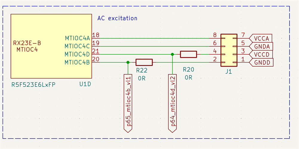
The crossed-out resistors are "do not populate". These LCD signals use the same pin as other functions on the board. I don't really need the resistors, if I don't plug the LCD in. But they are just empty footprints. The cost can be neglected.

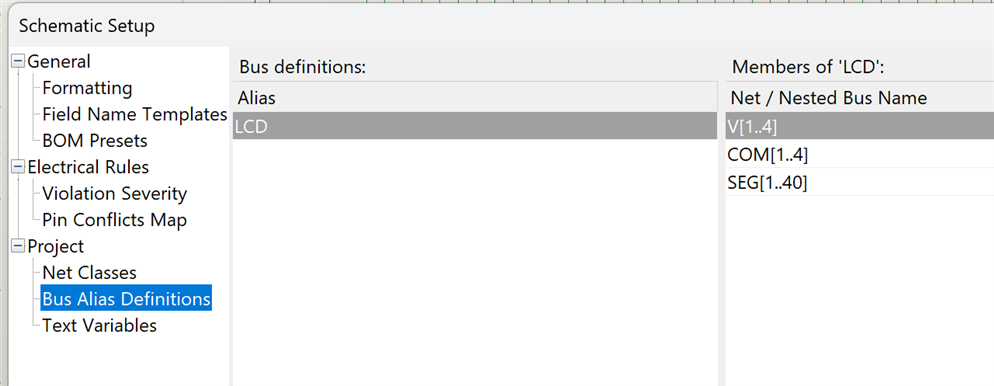
Using a BUS in KiCAD 8:

In early KiCAD, a bus didn't hold a lot of intelligence. It was a blue line where you could connect signals to. In newer KiCAD versions, this has changed. A bus has structure, and knows what signals it holds. It can be a combination of signals, or a range. In my case: both. The LCD bus holds 3 ranges of signals: 4 voltage pins, 4 communication pins, and 40 segment signals.

I first defined the bus in the schematic setup:

image

Then I routed signals from the microcontroller to the bus, and from bus to LCD connector. The wires are (have to be) labeled at both sides.

I used global labels to indicate those shared signals, because they are shared in other sheets of the design. Example: with the timer that I use for AC excitation:

image

  • Sign in to reply

Top Comments

  • shabaz
    shabaz 7 months ago in reply to Jan Cumps +1
    Looks very good. It is clear those signals are attaching to a bus with those 45-degree bends, and well-labelled too. Easy to understand!
  • shabaz
    shabaz 7 months ago in reply to Jan Cumps

    I think that's worthy of raising on the KiCad forum, in case there's a way (and if not, then a feature request). I too would like to use such a feature. For sure there's some effort involved to make the components that will be connected together will have their symbols created in that compatible fashion but it would be worth it for the clarity of the resulting schematic.

    • Cancel
    • Vote Up 0 Vote Down
    • Sign in to reply
    • More
    • Cancel
  • Jan Cumps
    Jan Cumps 7 months ago in reply to shabaz

    I don't think that KiCAD has support for it, but I'd like to see that a bank only has one pin (or a few pins) in a symbol. Maybe called bank14[0..xx], + some supporting pins. And the connection mechanism would be a bus instead of a wire ...

    Let's say that you have a RAM IC. The symbol editor requires you to draw all address pins and all data pins. Wouldn't it be useful if you could make a symbol with one address pin[0..4]; one data pin [0..15] and a few supporting pins like reset, write, latch, clock, power and ground? and that the data and address pins came out as a bus, with known signals?
    ADM's Vivado already shows memory that way in their block designs.

    • Cancel
    • Vote Up 0 Vote Down
    • Sign in to reply
    • More
    • Cancel
  • Jan Cumps
    Jan Cumps 7 months ago in reply to shabaz

    I can work with Renesas' style.
    I think that their style is not easy when you want to tell a story, explain particular aspects of a design.
    But they have a structure and system. And it works. 

    Most likely, the way they do it, matches the corporate EDA software package workflow, and needs less time (and creativity) to draw.
    I learn that by trying to draw an "organic" schematic, I spend a lot of time pondering, balancing. In an industrial setting, that may not be efficient.

    • Cancel
    • Vote Up 0 Vote Down
    • Sign in to reply
    • More
    • Cancel
  • shabaz
    shabaz 7 months ago in reply to Jan Cumps

    Think I much prefer the method you chose, to split up the symbol (although if they were just creating a simple breakout, then the symbol looking like the physical layout could make sense). Renesas boards seem to have a lot of configuration pads! One Renesas board I saw had them spread all over the board, and was very hard to locate the right ones.

    I never got around to completing this, but I split up a Spartan symbol in a similar manner.

    image

    • Cancel
    • Vote Up 0 Vote Down
    • Sign in to reply
    • More
    • Cancel
  • Jan Cumps
    Jan Cumps 7 months ago

    for reference: Renesas schematic style.

    The LCD connector:
    image

    The microcontroller (single symbol with all pins):

    image

    and the "patch bay":

    image

    • Cancel
    • Vote Up 0 Vote Down
    • Sign in to reply
    • More
    • Cancel
>
element14 Community

element14 is the first online community specifically for engineers. Connect with your peers and get expert answers to your questions.

  • Members
  • Learn
  • Technologies
  • Challenges & Projects
  • Products
  • Store
  • About Us
  • Feedback & Support
  • FAQs
  • Terms of Use
  • Privacy Policy
  • Legal and Copyright Notices
  • Sitemap
  • Cookies

An Avnet Company © 2025 Premier Farnell Limited. All Rights Reserved.

Premier Farnell Ltd, registered in England and Wales (no 00876412), registered office: Farnell House, Forge Lane, Leeds LS12 2NE.

ICP 备案号 10220084.

Follow element14

  • X
  • Facebook
  • linkedin
  • YouTube