


Table of Contents
Introduction
This blog post discusses how to create a custom component footprint in KiCad. There are different ways to do it; this blog post focuses on a popular scenario where the component has two rows of pins, enabling the use of a Wizard for speeding up the task. There are Wizards built into KiCad for a variety of popular scenarios, so it is worth checking them out, and being aware of how to use them and tweak the Wizard output to match your specific needs.
Getting Started
You’ll either need to find a CAD drawing of the component or manually measure it with (say) calipers. For this example, the component is an ESP32 development board, and it doesn’t come with a fully dimensioned drawing, and I don’t have a physical one to measure, so I had to fill in some of the unknown measurements with close approximations.

Next, from the KiCad applications launcher, click on Footprint Editor to launch it!
Create a Footprint Library and select 'Create Footprint'
Create a library to store your custom footrpints; I clicked on File->New Library and called it ESP32_Footprint_Library but you could create one with a more general purpose name such as User_Footprint_Library.
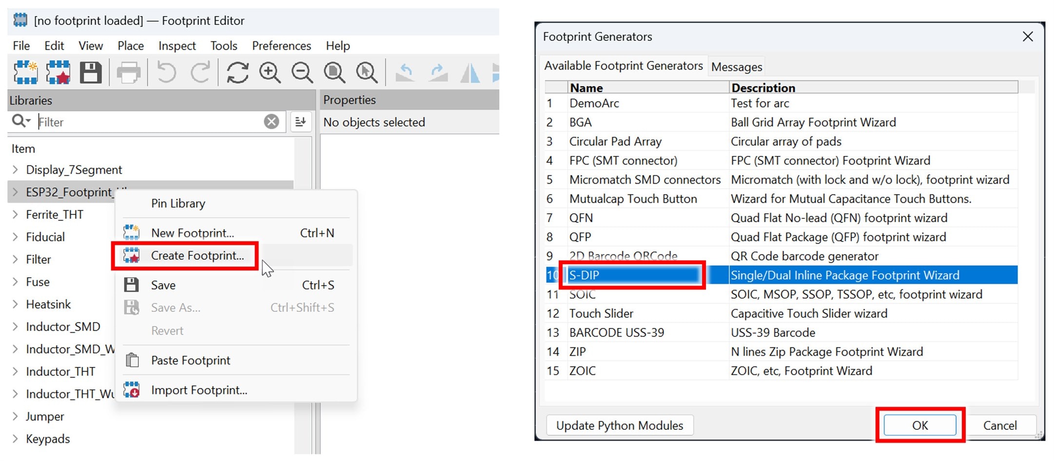
In the left pane, select your new library, and right-click on it. You’ll see a New Footprint menu option, but ignore that, and instead, select the next one, which is Create Footprint. The difference is, that New Footprint supplies a blank footprint drawing canvas, whereas Create Footrpint invokes a Footprint Generators wizard which will speed up the footprint creation.
Take a look at the wizard options, and select the most relevant one, which will be S-DIP, which is intended for Single-Inline or Dual-Inline Packages.
Footprint Generator Wizard
In the Footprint Wizard that was invoked as discussed above, you’ll see some categories (such as Pads and Body) on the left side, and then a load of parameters and their settings to the right of that. Work your way through that, modifying things to suit the component dimensioned drawing as best as possible.
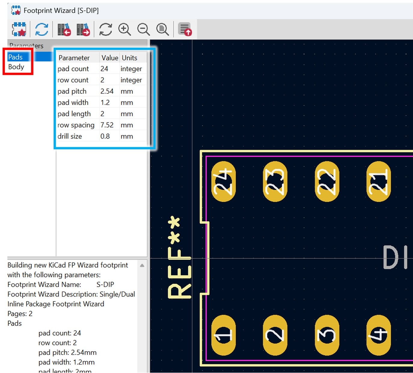
The Pads category for the S-DIP wizard is the most important. The Body category for S-DIP defines the silkscreen outline, and it’s not ideal, so I decided to let the Wizard do whatever it likes with the outline, and I can delete or edit that later.
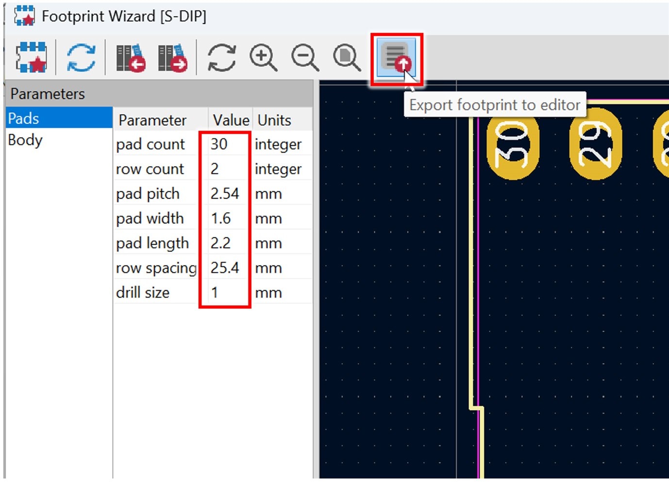
For the example ESP32 board, I populated the Pads category as shown in the screenshot below, and then clicked the Export footprint to editor icon.
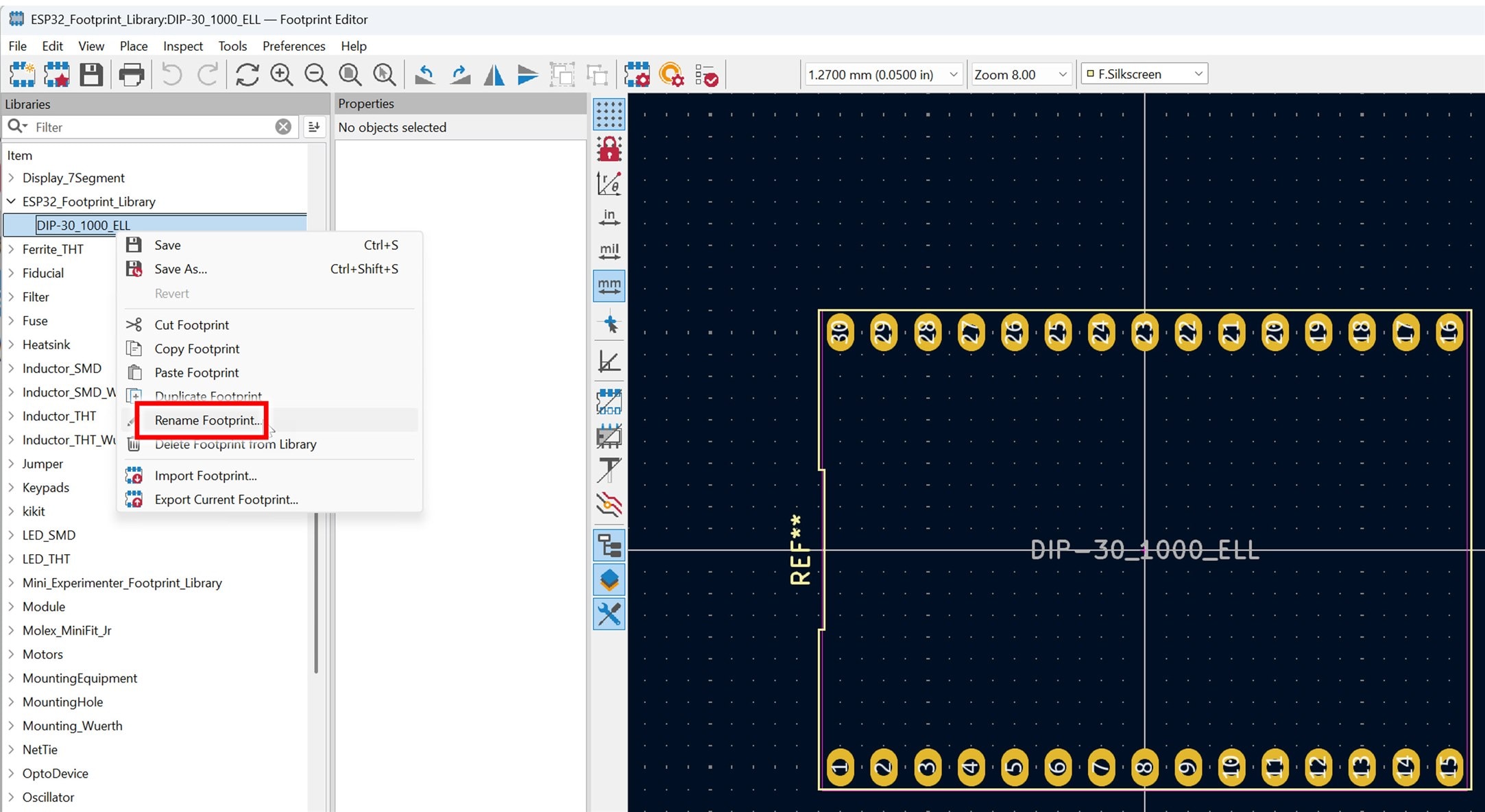
You’ll notice that the Wizard created the footprint with an unwanted name. Right-click on it, select Rename Footprint and give it a better name. With some versions of KiCad, there is the risk of accidentally overwriting old footprints you’ve created with new ones, so it’s important to always rename to something different to what the Wizard named it as.
Deleting Items
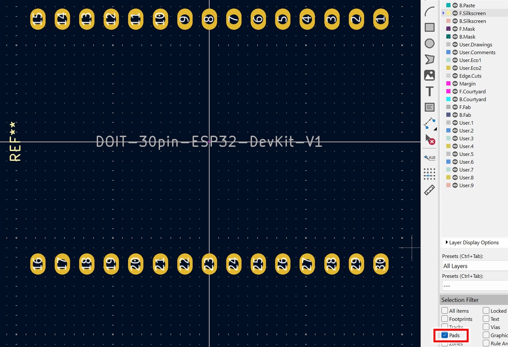
As mentioned earlier, the silkscreen from the Wizard wasn’t too good, so I decided to delete it, plus the Courtyard outline (this is discussed later). To do that, first look at the Selection Filter (it is present at the lower-right of the window) and you’ll see everything has a check-mark. Click on All Items, so that the check-marks are toggled to disappear. Then, select the Graphics check-box.
Next, click and drag inside the canvas area, to draw a blue shaded box around everything, then release the mouse. Only the graphics will be selected (i.e. silkscreen and courtyard).

Hit the Delete key on your keyboard, to delete those graphics. All that will remain is the text and the pads!
Don’t forget to click on All Items in the Selection Filter afterwards, so that everything there is check-marked as it was before.
Check Pads Numbering Direction
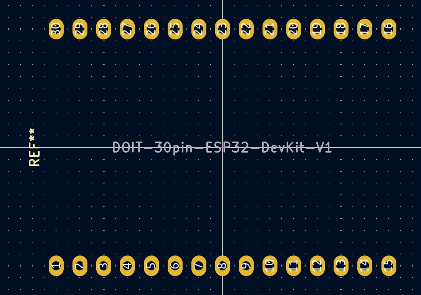
By default, the Wizard has laid out the pads to suit a typical DIP integrated circuit with pin 1 at the bottom-left. If that doesn't reflect the component you’re using, then the pads may need moving. In my case, it was easier if Pin 1 was at top-right to match the diagram that I had. It was easy to match that, by again clicking on All Items in the selection filter to deselect all, then selecting only Pads in the filter, then dragging to draw a shaded blue box over everything, then pressing R for Rotate twice. The result looked as shown here.
Click on All Items in the Selection Filter afterwards, so that everything there is check-marked as it was before.
Draw Silkscreen and Courtyard Outlines
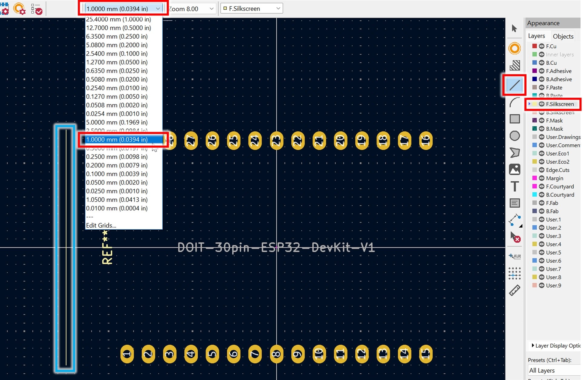
Next, roughly sketch one of the vertical silkscreen lines. To do that, first select a suitable grid (such as 1 mm), and select the F.Silkscreen (front silkscreen) layer from the right side pane, and select the Draw Line tool.
Click in the canvas once to set the starting point of the line, then move to the end point, and click again. Then, press Escape to stop the current line, and then press Escape a second time to quit the Draw Line tool.
You now have a line that is roughly in the desired position, but it needs to be made accurate as discussed next.
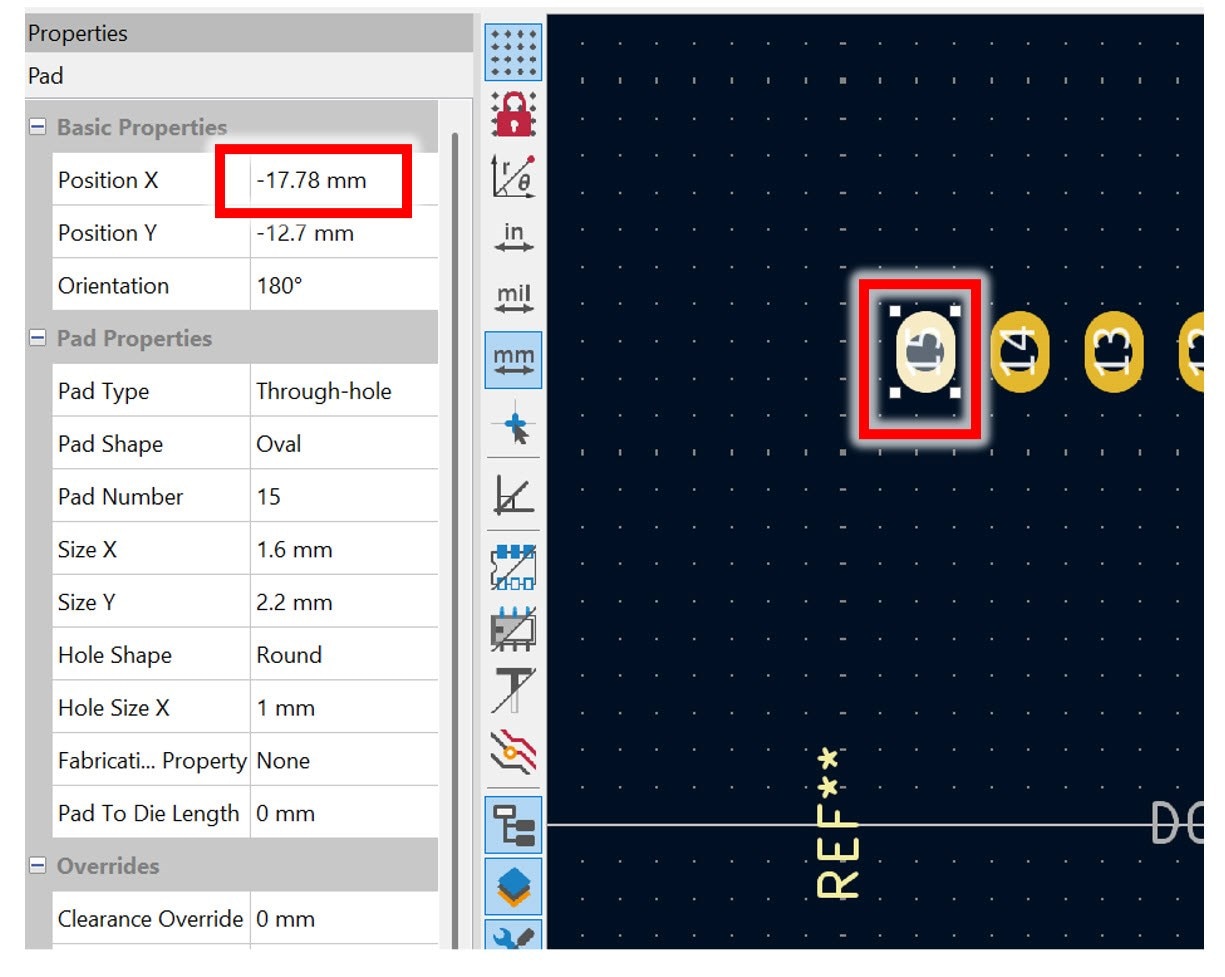
From the original component drawing, you can see that the line needs to be 28mm long and positioned 9.5mm to the left of the leftmost pads. Click on one of the leftmost pads, and see what its x-coordinate value is; you can read it off in the Properties pane on the left side of the canvas. If you don’t see any Properties pane, then you’ll need to enable it by clicking on View->Show Properties Manager.
As you can see in the screenshot below, the x-coordinate of the leftmost pad is -17.78mm.
Next, either single-click on the silkscreen line that you drew and then edit the values in the Properties pane, or, alternatively, double-click on the line and set the properties in the pop-up window.
For the x-coordinates, you can type -17.78-9.5 and KiCad will automatically perform the calculation.
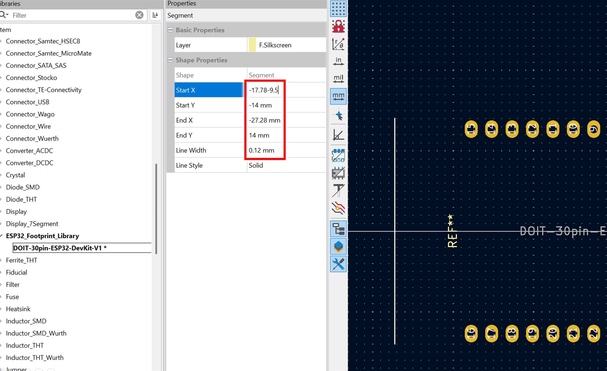
Since the line is symmetric about the x-axis, the y-coordinates were set to -14 and 14mm, since that’s a length of 28mm.
I made a mental note that the left silkscreen line now had an x-coordinate value of -27.28, because that’s needed for calculating the following part.
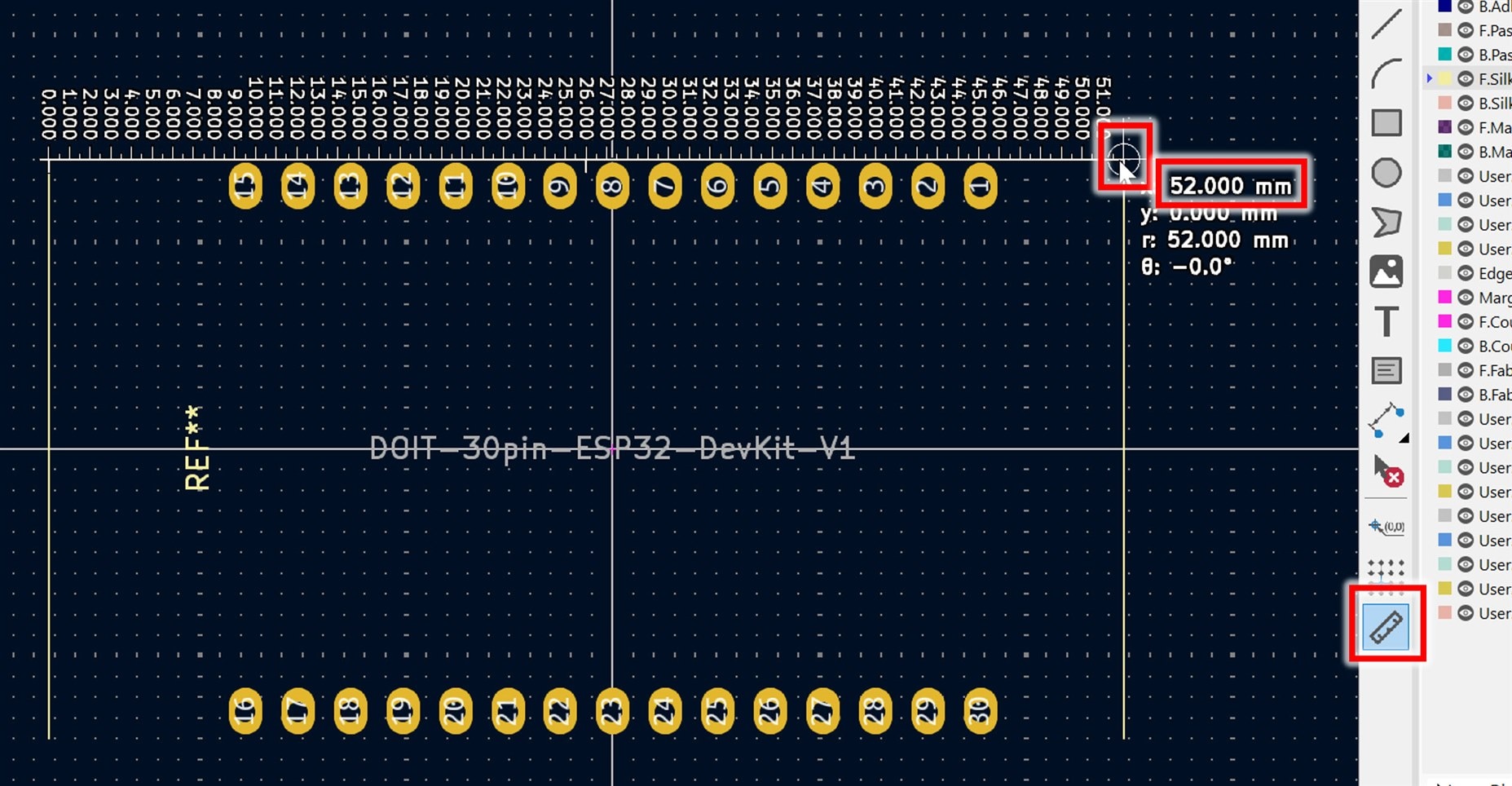
Next, I roughly drew the rightmost silkscreen line and then edited it such that the x-coordinate was -27.28+52, since the entire component has a dimension of 52mm.
You can check that things are correct by using the Measure tool in the palette on the right side of the canvas. Select it, then hover your mouse over one end of a line, and the cursor will turn into a circle with cross-hairs when it has snapped to the line endpoint geometry. Click with the mouse, then hover the mouse at the other line endpoint, and again you’ll see a circle with cross-hairs. You can read off the desired measurement to confirm that the two lines are spaced by 52mm.
The horizontal lines are easy; select the Draw Line tool as before, and now hover your mouse over a line endpoint as if you were still using the Measure tool. Again, you’ll see a circle with cross-hairs. Click once to set the line starting point, then move to the other line, and click to set the other end. Repeat this and you’ll have a box shape drawn! Note that you could have used the Draw Rectangle tool instead of the Draw Line tool, but sometimes component outlines are complex and the Draw Line tool is a bit more flexible.
You could tweak further as desired. I decided not to draw the horizontal lines fully from side to side, because the pads are too close to the edges.
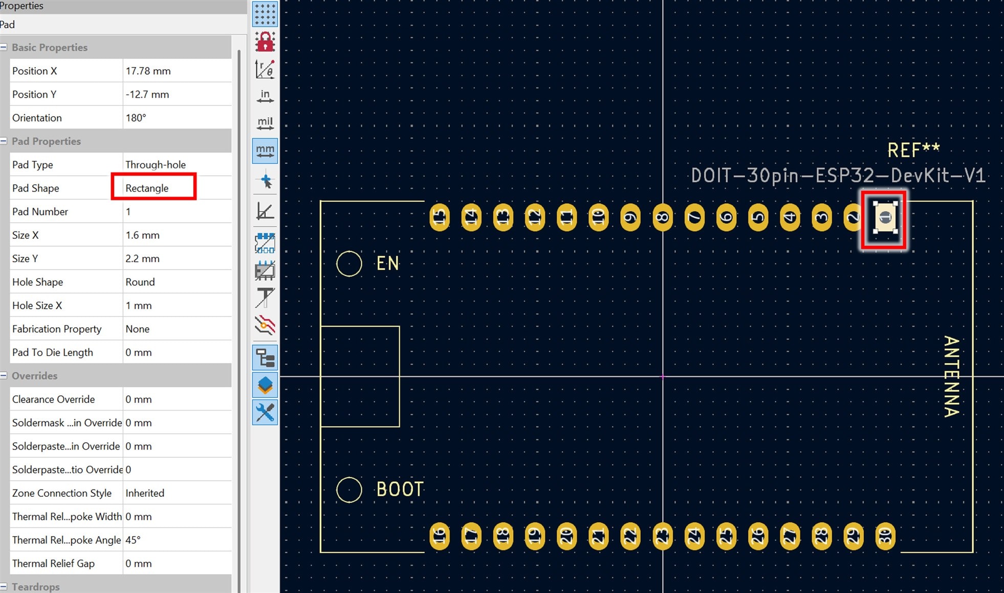
I used the Add Text tool and the Draw Circle tool in the example here. Also, since it is customary to set pin 1 to be a different shape pad, I clicked on that pad once, and then changed the Pad Shape attribute in the Properties pane, to Rectangle.
I used the M and R keys to Move and Rotate the text shown in the screenshot below.
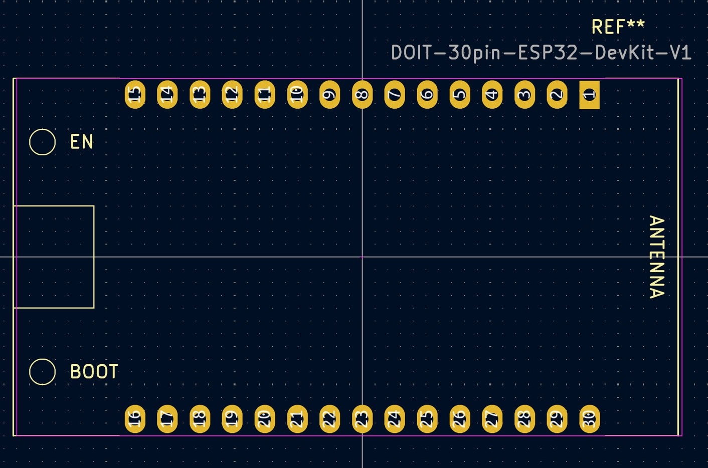
The Courtyard is used to roughly define the limits of the component outline, so that the PCB error check can flag an alert if two components are placed accidentally overlapping each other when it comes to the PCB layout. Select the front courtyard (F.Courtyard) layer from the layers pane on the right of the window, and then select the Draw Rectangle tool, and draw a rough outline.
You could make it more accurate for critical applications. I didn’t bother.
Keepout Rule Areas
Technically, since there is an antenna, you should also use the Rule Area tool from the palette on the right side, to outline the antenna area such that no pads or copper planes get placed there during the PCB layout, without errors being flagged.
It would be even better to simply place the component protruding from the PCB edge, but that’s another story, which we can skip for the purposes of this simple tutorial.
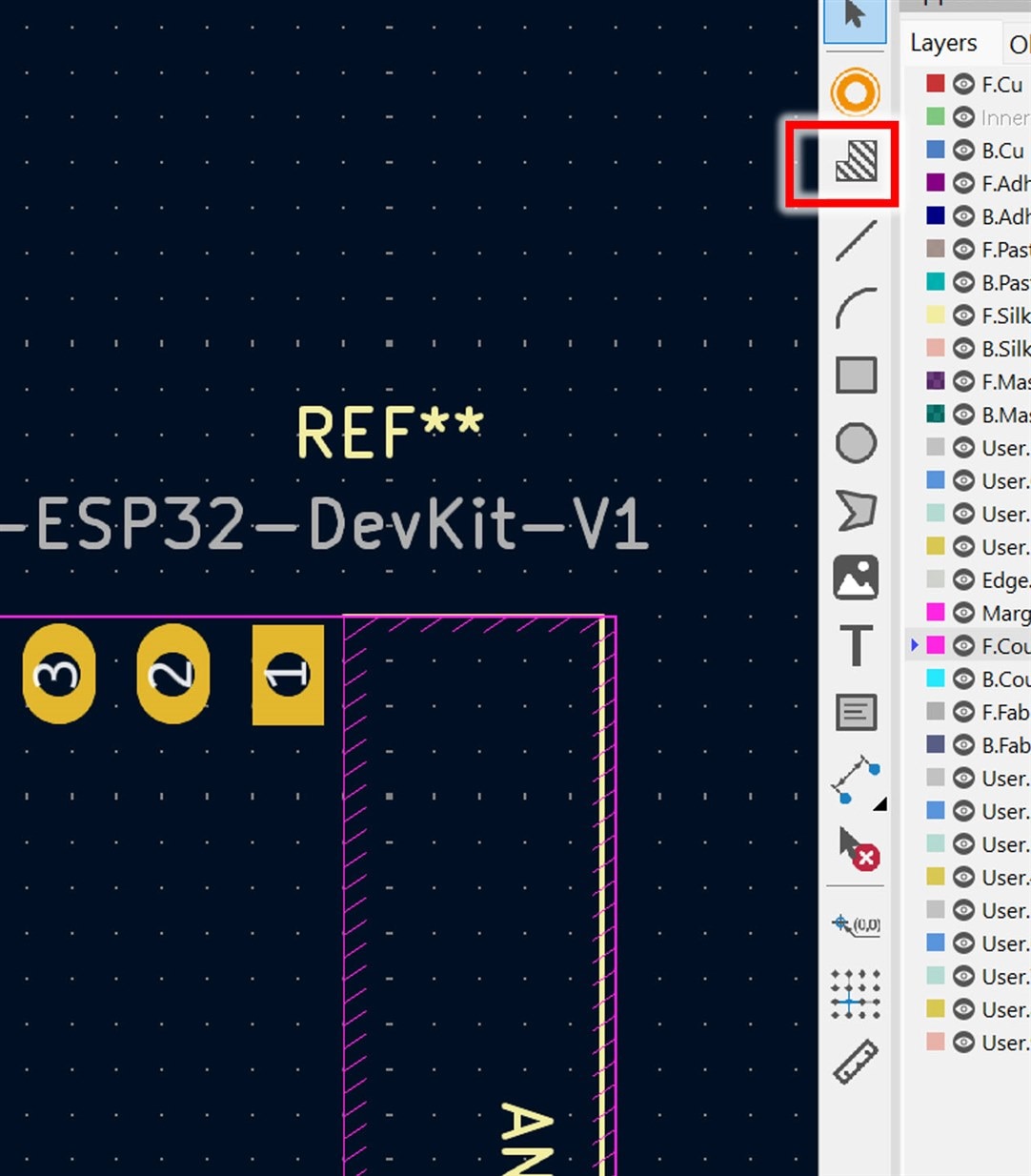
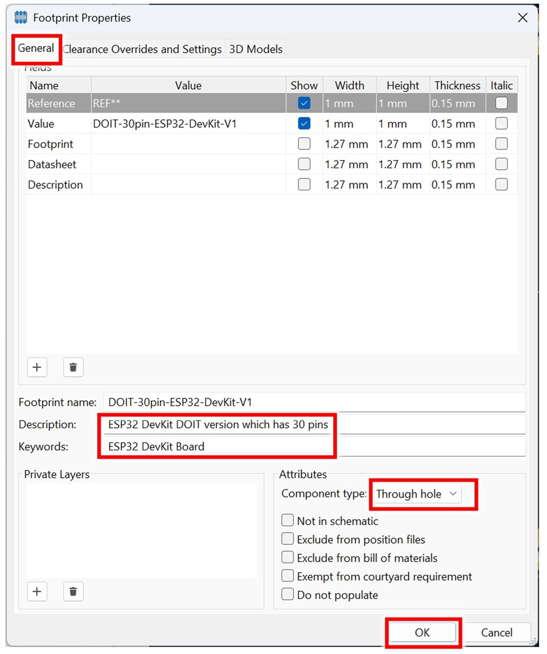
Footprint Properties
Click on File-> Footprint Properties and populate what you can. The screenshot here shows what I normally populate at a minimum.
At this stage, you are pretty much done with the component footprint! Press Ctrl-S to save it, although you should have been doing that periodically, just in case the software or the PC crashes.
Check your work with 3D Models
If you can manage to find a 3D model of the component, it’s highly recommended to configure it using the Footprint Properties (as shown in the screenshot above, but this time clicking on the 3D Models tab in that window). The reason is, it can help to verify the footprint.
I found an ESP32 board 3D model on the Internet, and while it is not an exact match for the ‘DOIT’ brand ESP32 board, it was good enough, and it showed me that I should enlarge the silkscreen outline slightly, which I did.
Now I’m fairly confident the footprint would be suitable.

Check my work
If you wish to try out the footprint that was created for this tutorial, you can find it zipped up further below; extract the zip file somewhere on your PC.
To use the extracted footprint file, go to the Footprint Editor, and then ensure you have a library created (create a library using File->New Footprint Library), and then click on File->Import->Footprint and select the file on your PC. You’ll see the footprint appear in the canvas area. Next, select File->Save and choose the destination library to save it in. Some versions of KiCad are buggy and File->Save might not work, in which case try to close the Footprint Editor, which should prompt to save first.
Summary
Creating footprints can be accelerated by using a Footprint Generator Wizard and plugging in values off the component drawing from a datasheet if possible.
Next, ensure the pin numbering order matches the component drawing, and then you can adjust the component silkscreen and courtyard outlines as desired. The Footprint Properties window is used to set some basic attributes for the component, and it also allows a 3D model to be associated with the footprint, which can help verify that the footprint was created accurately.
Thanks for reading!


