


Table of Contents
Ever seen a component you wish to use with KiCad, but you can’t find an existing symbol anywhere? It’s easy to create a custom symbol!
Getting Started
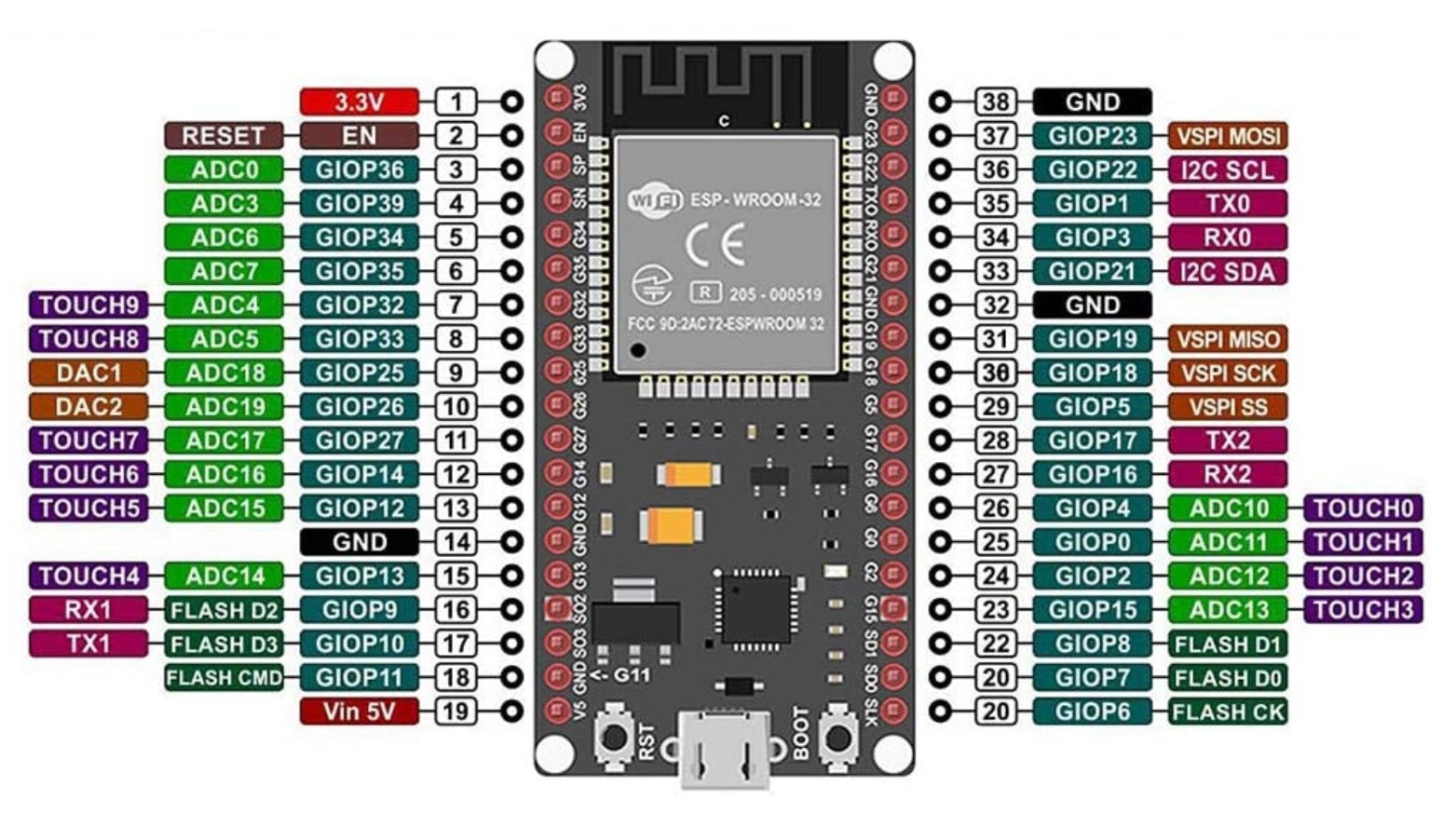
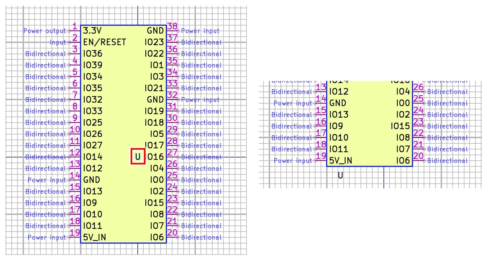
First off, find a diagram you can work from:
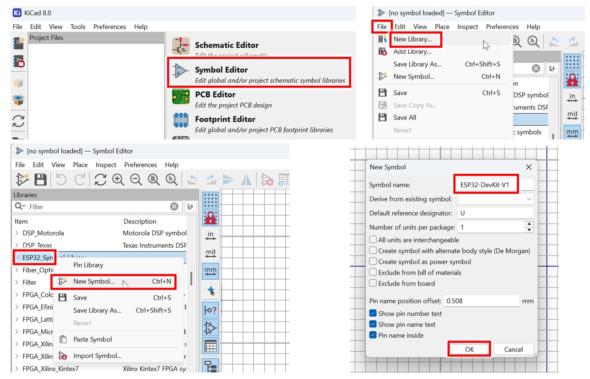
Next, from the KiCad applications launcher, click on the Symbol Editor, to launch it!
Create a Symbol Library and New Symbol
Create a library to store your custom symbols; I clicked on File->New Library and called it ESP32_Symbol_Library but you could create one with a more general purpose name such as User_Symbols_Library.
Now you’re ready to create a symbol within your library. Right-click on the library name that you just created, and select New Symbol, and give it an appropriate name. You can see all the steps in the screenshots here:
Create Pins, Slow method and Fast method
Now you’re ready to create all the individual pins for the symbol! There are several ways to do this, I’ll demonstrate the tedious way first.
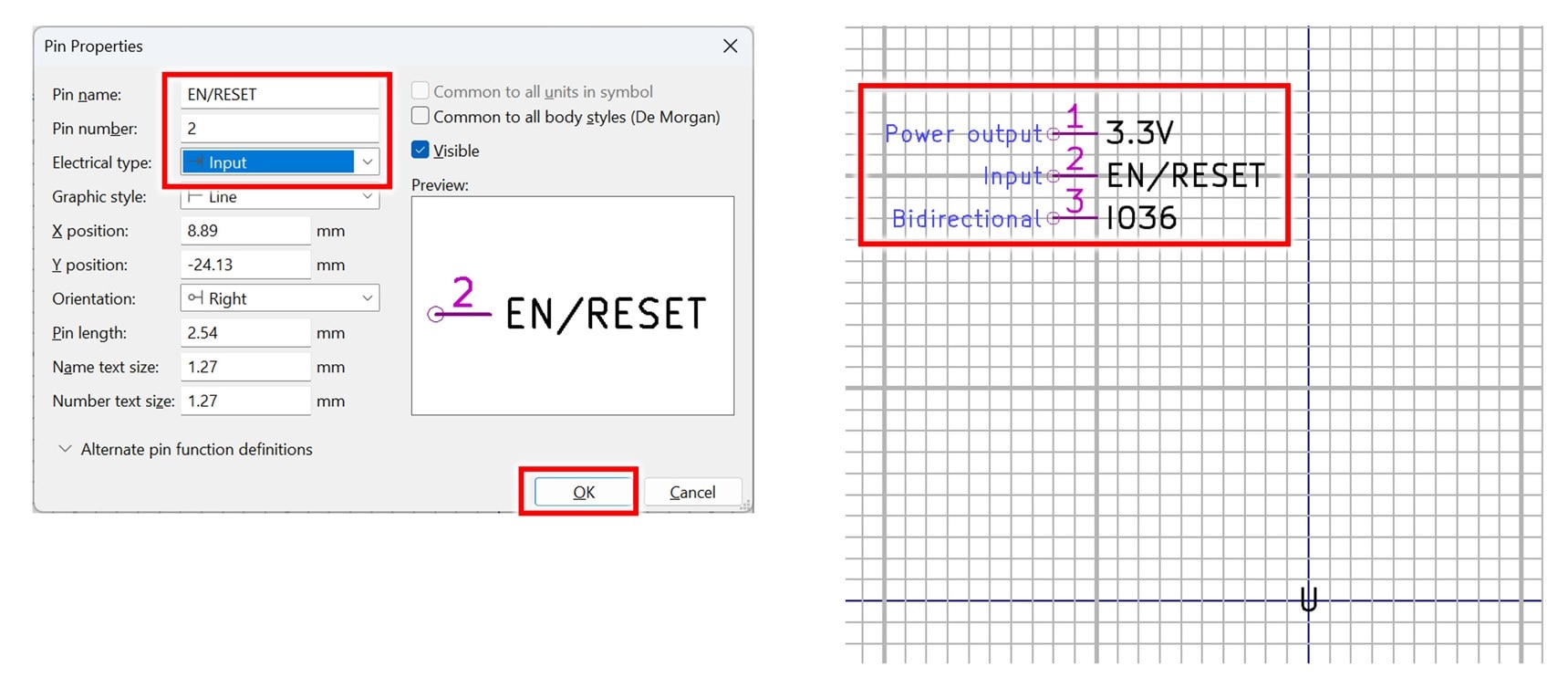
Double-click on the new symbol name you just created to make sure it is selected. Then, click in the canvas area and type ‘P’ to add a pin. From the earlier diagram, you know that pin 1 is a 3.3V power output pin, so that’s what you need to populate in the Pin Properties window, then press OK.

A pin will be attached to your cursor, just set it down anywhere on the canvas. Then hit ‘P’ again, to move on to the next pin, which is RESET/EN pin 2.
After you’ve done this a few times, your canvas will look as shown in the screenshot below. You can see that the EN/RESET pin was set as an input, and then the next pin (GPIO36) was set to Bidirectional since we don’t know how the user will configure that pin in the microcontroller code.
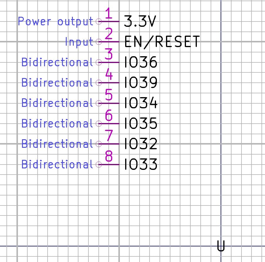
There are a lot of GPIO pins, but for a slight speed-up, just copy-paste the GPIO pin on the canvas, and then double-click each one to edit the pin number and GPIO name. Here’s what it will look like after a while:
If you’re getting fed up doing this, then click on Edit->Pin Table to see the following window. Notice it contains all the pins you’ve created so far.
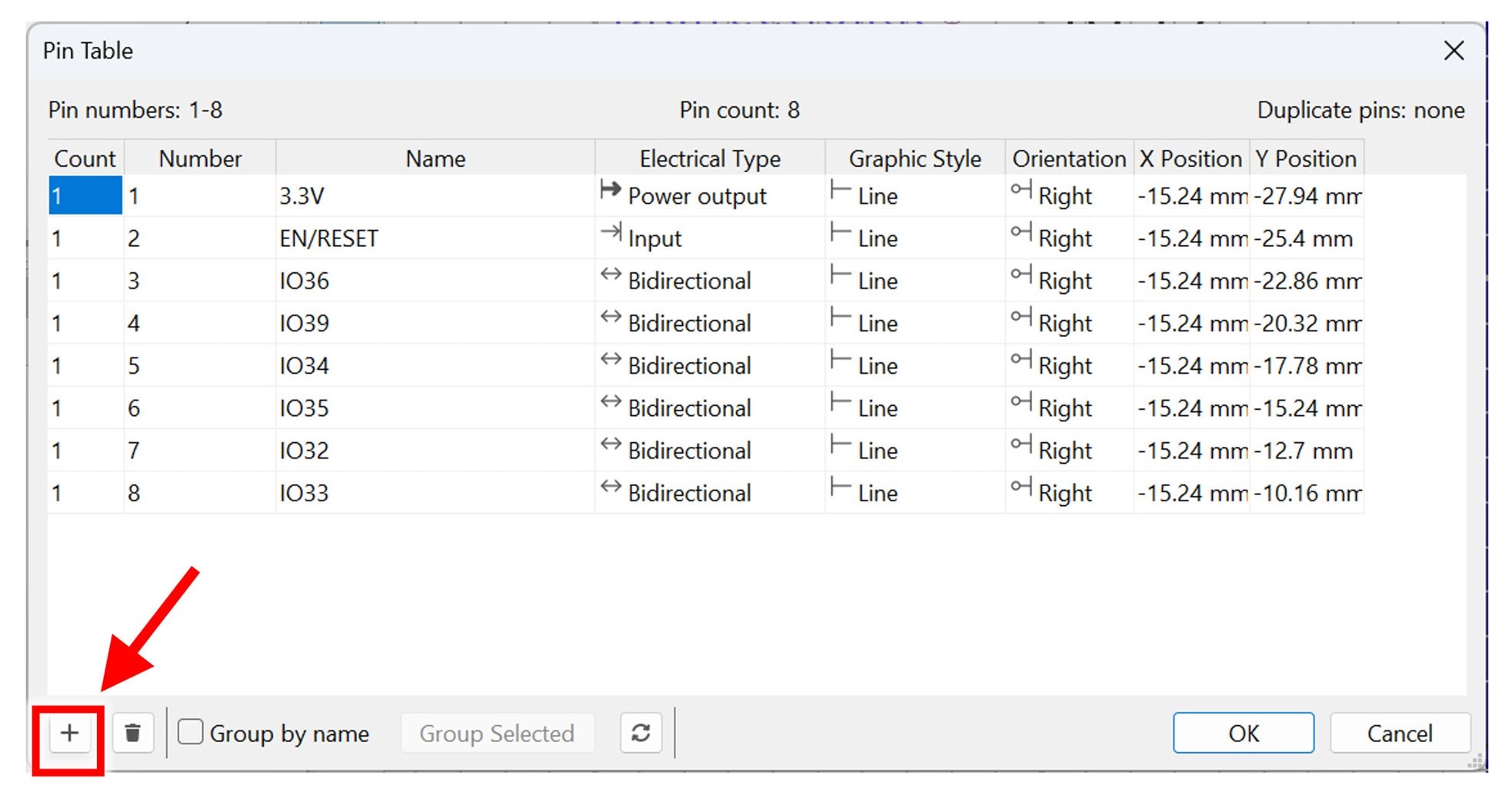
Now it’s far quicker. All you have to do is click on the add button highlighted in the screenshot above, and you’ll see a new row appear, with the Number column selected. Type the next pin number there, then press Tab, and the Name column will be highlighted. Type the pin name, and press Tab again. You don’t need to change anything else, so now press Enter, and you’ll see the row is accepted, and the cursor in on the following row Number column. Keep repeating, pressing Tab to step horizontally, and Enter to create a new row. You may need to change from Bidirectional to (say) Power Input or some other selection, when you reach pins that are not GPIO.
Eventually you’ll have a long list! Press OK and you’ll see it all dumped on the canvas.
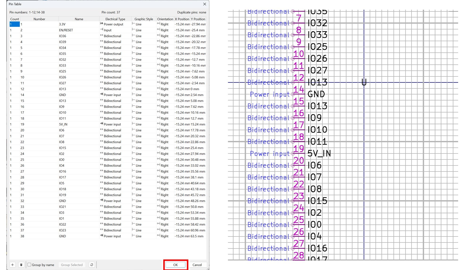
Using that Pin Table method, you’ll be done within five minutes even for a symbol with as many pins as this example has.
If you’ve made mistakes, don’t worry; either try to edit the pin table if that’s what you’ve got open, or, you can always add (by pressing ‘P’) or edit pins (by double-clicking them) directly on the canvas whenever you spot a mistake.
Rearrange Pins
The symbol is currently just a long column of pins on the canvas. To make a decent symbol, we need to move some pins, which entails selection.
Click and drag to draw a shaded pink box around the pins you wish to move. We know the symbol has 19 pins on each side, so I want to move pins 20 to 38 in this example. When you have drawn the pink shaded box, release the mouse button, and you’ll see the selected items have a blue glow around them.
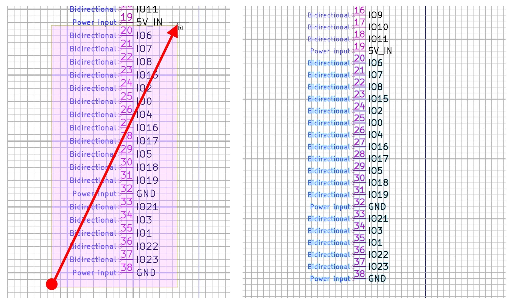
Now you can press ‘M’ to move, and all the selected items will be attached to the mouse pointer. Press ‘R’ twice to rotate the pins by 90 and then 180 degrees, then once you’re happy with their position, click to drop the items onto the canvas.
Check your Work
It’s good to visually scan the diagram you’re using as a reference, and double-check you’ve also got all the pins numbered the same, and that all the pin names are appropriate. I count each pin number, to make sure I’ve not missed a pin, or double-entered a pin, and then I check each pin name.
Drawing a Box and Symbol Properties
It’s now going to look more like a symbol! Click on the rectangle icon on the right-side palette, then click once at the top-left where you want one corner, and then click once at the desired bottom-right location, and a rectangular shape will be drawn in blue. Hit the Escape key to exit the rectangular box creation mode. Then, double-click on the box you’ve just drawn, and a properties window will appear. Type 0.254 for the width (this is the standard width for KiCad style component symbol outlines) and then select that you wish the box to be filled with the standard background color for symbols. Then click OK.
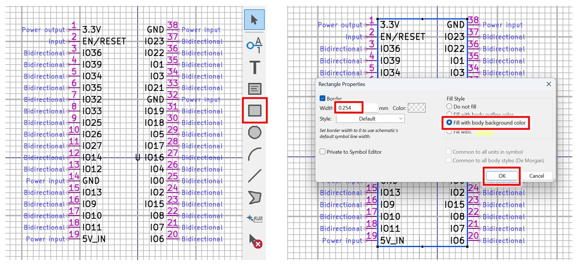
Click anywhere on the canvas away from the symbol, to deselect the rectangle, and you’ll see that the color will be yellow. The symbol is almost complete. Notice the ‘U’ which is the component reference designator, is in the wrong position. Click once on it to select it, then press M for move, and then move your cursor to position it somewhere more sensible, then click on the mouse to drop it into position.
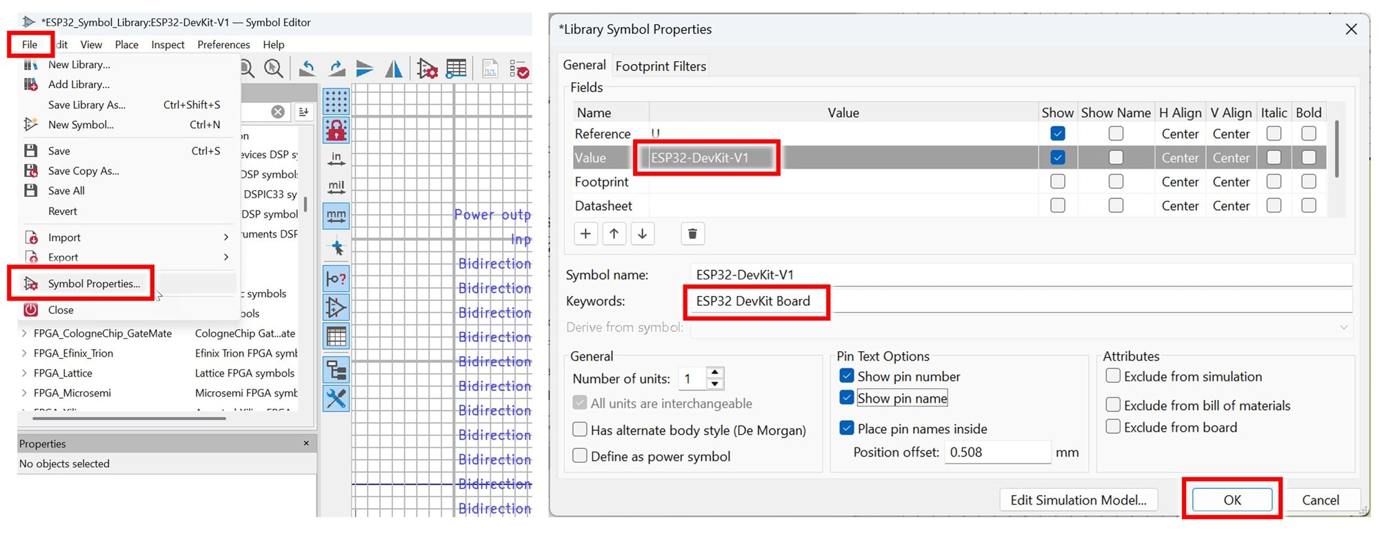
You’re on to the last bits of the symbol creation process now. Go to File->Symbol Properties, and fill in any fields you can. I typically just fill in the highlighted fields below.
Finally, press Ctrl-S to save the symbol! (ideally you should have been saving at regular intervals as you went along too, just in case of a software or PC crash).
The symbol is now ready for use within KiCad schematics.

Consider Symbol Usability
If you think about it, the created symbol isn’t always ideal, because it contains several ground pins buried between GPIO pins, which will make it awkward to draw a decent schematic. The solution is to create a more logical layout that doesn’t necessarily match the physical component.
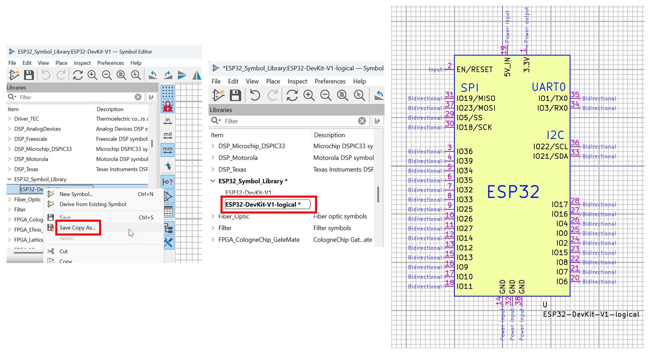
To do that, right-click on your symbol in the left-side pane in the Symbol Editor, and select Save Copy As. Type a name such as ESP32-DevKit-V1-logical.
Next, double-click on the new name in the left pane, so that you’re not accidentally modifying the original symbol that you created.
Now you could move pins around, and, for instance, place all the GND pins at the bottom of the symbol (use the M and R keys to move and rotate), and the supply pins at the top. You could also double-click the pins and edit the names to better reflect how you wish to use them. In the screenshot below, I renamed some pins to indicate that they can be used for I2C, SPI and UART.
Use the Text icon in the right-side palette to add some annotations to parts of the symbol if it helps.
Check my Work
The symbol library will be stored in a location such as C:\Users\your_user_name\Documents\KiCad\version_number\symbols and will be called ESP32_Symbol_Library.kicad_sym if you used the same library name as I did.
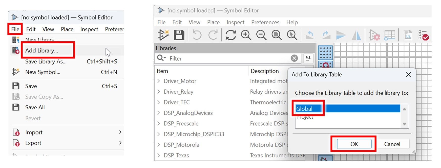
I’ve zipped up and placed the ESP32 symbol library as an attachment to this blog post further below. If you wish to use it, unzip it, and place it at the location mentioned ( C:\Users\your_user_name\Documents\KiCad\version_number\symbols ) and then within the Symbol Editor, click on File -> Add Library, then select Global, then select the file.
Another way to do the same thing is to select Preferences -> Manage Symbol Libraries in the Symbol Editor.
Video
For a video demonstration of symbols being created (using the slow method), see the following (forward to 8 minutes 30 seconds for the discussion on symbols):
Summary
Creating a new symbol for KiCad entails creating a user symbol library (if you don’t already have one created by yourself before), and then adding a new symbol definition into it. Then, you can drop pins onto the canvas, or bring up the Pin Table for speedily adding many pins to the symbol. You can select, move and rotate pins, and then draw a rectangle and style it to look like a component symbol. Finally, you edit the Symbol Properties with a few symbol attributes and then save your work, and you’re good to go.
The symbol library that was created is attached below (unzip it and then follow the directions in the Check My Work section above).
Thanks for reading!
Top Comments