


Introduction
The purpose of this blog is to analyse the advantages of placing circuits into a printed circuit board (PCB), and show the design process to make the PCB compatible with the hardware components which are mentioned in the first blog. First of all, a PCB acts as mechanical support to hold the electronic circuit. One of the most common materials used to create a PCB is FR4 (epoxy resign fibreglass), and its thickness is often determined to be 1.6 mm. In addition, the board is coated in a copper layer which is etched way to leave the tracks behind, and its thickness is defined in oz/ft2
1 oz/ft2 = 35 μm
Furthermore, the simplest form of a PCB is a single-layer PCB. Copper is placed only at the bottom of the board. Holes are drilled through the material, so components are placed at the top and soldered at the bottom. A more complicated form of PCB is a double-layer PCB, which is used in this project. Copper is placed at both sides of the board, and components can be mounted at the top and the bottom. Tracks can also be on both sides, and plated through holes (vias) are used to allow higher density of routing. Finally, even more complex are the multi-layer PCBs. Up to 32 layers of copper could be connected through vias to create small, high density routing circuits.
Advantages of PCB
Nowadays, the printed circuit board is certainly an excellent invention in electronic circuit design. The use of PCBs provides many advantages compared to using prototype boards. Firstly, all components in a PCB are fixed. Components are soldered instead of being connected through wires. Another important advantage is that connection errors and short circuits are eliminated since PCBs are designed in software, where electrical rule check and design rule check are applied before production. Furthermore, the cost of PCB mass production is lower than manually created boards just by the re-use of a PCB schematic.
PCB Design in Eagle
Schematic
To begin with, the software used to design the PCB was EAGLE. A new project was created and a third-party was added which would allow the use of the desired components. To continue, a schematic was created where components were connected together. The wiring tool which was used was the ratsnest. This tool is very useful when designing a PCB because it provides a visual feedback in the board design of the connections that should be routed. The drawn schematic is shown in the figure below:
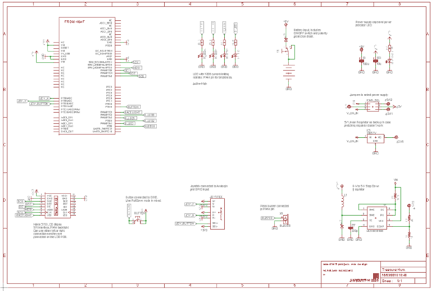
It is noticeable that components are connected through labels instead of wires. This is a convenient function of EAGLE to maintain the schematic well structured and easily readable. Finally, an electrical rule check is applied to check for errors between connections.
Board
Once the schematic is finished the switch to board function is used where the routing takes place. One of the most important things when designing a PCB is to put the components down in a logical manner. Furthermore, tracks must be as nice and neat as possible. A famous quote of professional PCB designers is:
“If it looks good, it works good.”
Another important thing to keep in mind, is that small distance must be kept between pads as the should not overlap with each other. In addition, polygons are added to the top and the bottom of the PCB which connect all grounds together. In this design polygons are placed on top of each other. The complete PCB design is shown in the figure below:
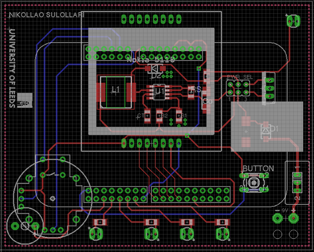
Finally, a design rule check was applied to check for errors in the design. Once it is assured that the design is correct is recommended to do another chek of the schematic and the PCB before it is sent for manufacture.
Conclusion
To take everything into account, the aim of the blog was to demonstrate the PCB design of this project, and discuss some advantages of the use of PCBs compared to prototype boards. The next part of the project would be to write the code which would implement the game by interacting with the hardware.