element14 Community
element14 Community
    Register Log In
  • Site
  • Search
  • Log In Register
  • Community Hub
    Community Hub
    • What's New on element14
    • Feedback and Support
    • Benefits of Membership
    • Personal Blogs
    • Members Area
    • Achievement Levels
  • Learn
    Learn
    • Ask an Expert
    • eBooks
    • element14 presents
    • Learning Center
    • Tech Spotlight
    • STEM Academy
    • Webinars, Training and Events
    • Learning Groups
  • Technologies
    Technologies
    • 3D Printing
    • FPGA
    • Industrial Automation
    • Internet of Things
    • Power & Energy
    • Sensors
    • Technology Groups
  • Challenges & Projects
    Challenges & Projects
    • Design Challenges
    • element14 presents Projects
    • Project14
    • Arduino Projects
    • Raspberry Pi Projects
    • Project Groups
  • Products
    Products
    • Arduino
    • Avnet & Tria Boards Community
    • Dev Tools
    • Manufacturers
    • Multicomp Pro
    • Product Groups
    • Raspberry Pi
    • RoadTests & Reviews
  • About Us
  • Store
    Store
    • Visit Your Store
    • Choose another store...
      • Europe
      •  Austria (German)
      •  Belgium (Dutch, French)
      •  Bulgaria (Bulgarian)
      •  Czech Republic (Czech)
      •  Denmark (Danish)
      •  Estonia (Estonian)
      •  Finland (Finnish)
      •  France (French)
      •  Germany (German)
      •  Hungary (Hungarian)
      •  Ireland
      •  Israel
      •  Italy (Italian)
      •  Latvia (Latvian)
      •  
      •  Lithuania (Lithuanian)
      •  Netherlands (Dutch)
      •  Norway (Norwegian)
      •  Poland (Polish)
      •  Portugal (Portuguese)
      •  Romania (Romanian)
      •  Russia (Russian)
      •  Slovakia (Slovak)
      •  Slovenia (Slovenian)
      •  Spain (Spanish)
      •  Sweden (Swedish)
      •  Switzerland(German, French)
      •  Turkey (Turkish)
      •  United Kingdom
      • Asia Pacific
      •  Australia
      •  China
      •  Hong Kong
      •  India
      • Japan
      •  Korea (Korean)
      •  Malaysia
      •  New Zealand
      •  Philippines
      •  Singapore
      •  Taiwan
      •  Thailand (Thai)
      • Vietnam
      • Americas
      •  Brazil (Portuguese)
      •  Canada
      •  Mexico (Spanish)
      •  United States
      Can't find the country/region you're looking for? Visit our export site or find a local distributor.
  • Translate
  • Profile
  • Settings
PCB Design, Prototyping and Production
  • Products
  • More
PCB Design, Prototyping and Production
PCB Blogs Raspberry Pi RP2350 based PCB design
  • Blog
  • Forum
  • Documents
  • Leaderboard
  • Files
  • Members
  • Mentions
  • Sub-Groups
  • Tags
  • More
  • Cancel
  • New
Join PCB Design, Prototyping and Production to participate - click to join for free!
  • Share
  • More
  • Cancel
Group Actions
  • Group RSS
  • More
  • Cancel
Engagement
  • Author Author: embeddedguy
  • Date Created: 19 Jun 2025 8:16 AM Date Created
  • Views 2552 views
  • Likes 10 likes
  • Comments 16 comments
  • pcb
  • raspberry pi
  • rp2040
Related
Recommended

Raspberry Pi RP2350 based PCB design

embeddedguy
embeddedguy
19 Jun 2025

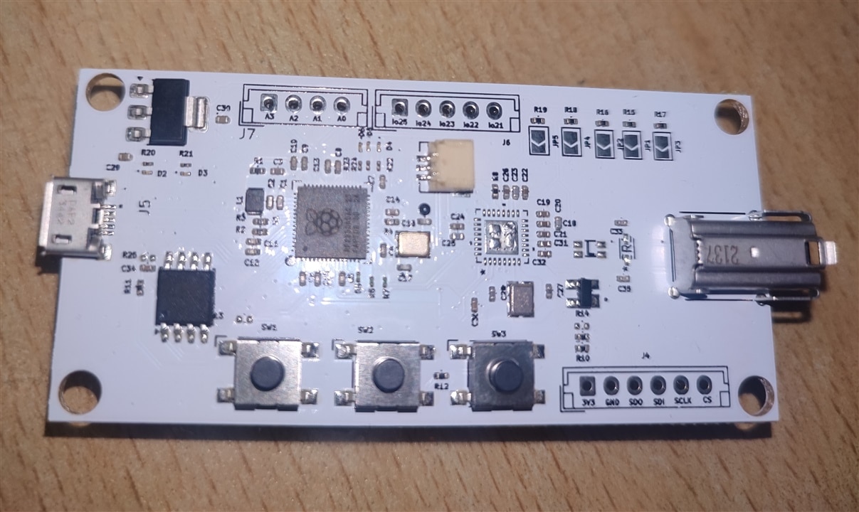
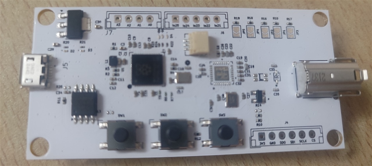
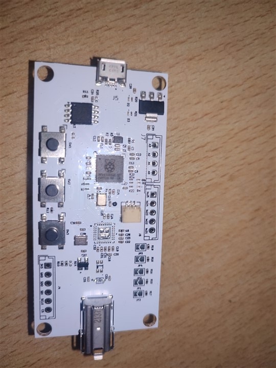
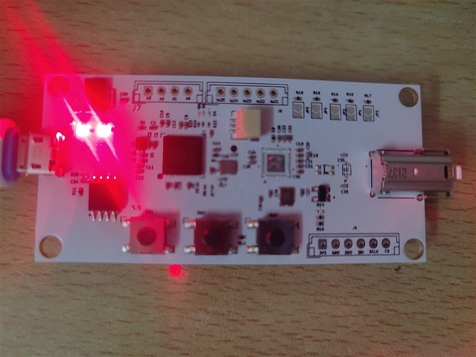
Sometimes back, I was designing a PCB based on RP2350 and now I received the finished PCB. So this post is about the experience that I would like to share about my PCB design.

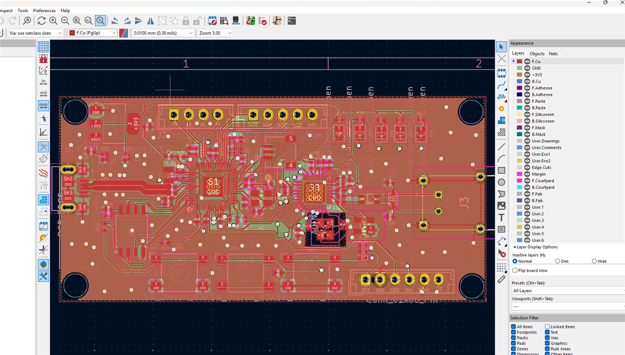
Firstly, the original plan of creating this PCB was to create RP2350 based Single Pair Ethernet development board. For that I had used ADIN-1111 chip. Unfortunately, it was not available during the PCBA making. Hence the original idea was not possible. But I have tested the RP2350 chip and it is working fine.  The design is based on KiCAD and is 4-layer design.

The easiest idea to test this board is to use Micropython so that the board can be tested fast. I tested a simple blink program on this board and it works fine.

image

image

imageimage

image

You don't have permission to edit metadata of this video.
Edit media
x
image
Upload Preview
image

  • Sign in to reply

Top Comments

  • BigG
    BigG 8 months ago +1
    Very nice. Does your SPE board include PoDL (power over data lines)? That's a design challenge just on it's own. I've always fancied the microchip SPE ICEs over ADIN-1111, purely on price. I see Arduino…
  • wolfgangfriedrich
    wolfgangfriedrich 8 months ago in reply to BigG

    And the board looks like it has paste already on the un-populated pads. To mount the chip it would need some flux, good enough placement and sufficient heat for assembly. 

    • Cancel
    • Vote Up 0 Vote Down
    • Sign in to reply
    • More
    • Cancel
  • BigG
    BigG 8 months ago in reply to embeddedguy

    You're right. They don't offer 10BASE-T1L chipset.

    I know TI do, and there's some nice reference material available online too. Wurth Eletronik, for example, also created a reference design based on TI chip.

    www.we-online.com/.../DP83TD510E-DP83TD510E-EVMl-LAN-POE

    • Cancel
    • Vote Up 0 Vote Down
    • Sign in to reply
    • More
    • Cancel
  • michaelkellett
    michaelkellett 8 months ago in reply to embeddedguy

    For future reference it is possible to hand solder (using a soldering iron) QFN parts like the ADIN chip.

    The trick is to make a footprint with a single large hole for the big centre pad. Make the hole as big as you can without breaking out of the pad.

    To solder the chip, apply solder past with a small pointy thing (I would use a needle in a holder)  - it doesn't matter if the paste bridges the outer pads but try not to bridge from the signal pads to the centre. Don't put any paste on the centre pad.

    Use a spring ar of some kind (I use a bit of bent "piano" wire held in a tiny vice) to hold the chip in place on the board and reflow the paste on the outer pads with a hot and very fine tipped soldering iron. It will need to be hot to get any heat down a really fine needle tip. Don't worry about bridging outer pads or soldering all of them.

    Once the paste has all been melted apply a lot of really runny flux (I use Warburtons 315))

    image

    You can get this from Rapid Electronics.

    Touch up the solder on the outer pads to solder any that are not and remove bridges. If there is too much solder remove some with solder wick. Keep it fluxy !

    Then solder the chip centre pad (if a connection is needed) using a bigger iron bit and some wire solder.

    Don't solder the centre pad unless you have to !

    The big centre hole concept is useful for removing chips even if you have a full reflow set up. Only do the multiple tiny holes thing if you need them for RF or thermal purposes.

    Obviously this isn't the ideal way to do things but if you need to add a QFN part after the rest of the board has been re-flowed it's the best cheap way I know. It can, of course, be done better if you have a fancy rework machine costing many £k and all the required add ons.

    It may help solder a QFN if you apply hot air to the underside of the board and get it up to about 120C.

    It is much, much easier to do all this with leaded solder - the unleaded stuff doesn't flow so well and has a much higher melting point.

    You can get ultra low melting point solder which might be even better but I have not tried it.

    MK

    • Cancel
    • Vote Up 0 Vote Down
    • Sign in to reply
    • More
    • Cancel
  • embeddedguy
    embeddedguy 8 months ago in reply to BigG

    Single-Pair Ethernet (SPE) PHYs Products Parametric Search

    • Cancel
    • Vote Up 0 Vote Down
    • Sign in to reply
    • More
    • Cancel
  • embeddedguy
    embeddedguy 8 months ago in reply to BigG

    Right. Thanks for this nice suggestion. 
    I will keep making PCBs and next time I will try to get when ordering the PCB.

    • Cancel
    • Vote Up 0 Vote Down
    • Sign in to reply
    • More
    • Cancel
<>
element14 Community

element14 is the first online community specifically for engineers. Connect with your peers and get expert answers to your questions.

  • Members
  • Learn
  • Technologies
  • Challenges & Projects
  • Products
  • Store
  • About Us
  • Feedback & Support
  • FAQs
  • Terms of Use
  • Privacy Policy
  • Legal and Copyright Notices
  • Sitemap
  • Cookies

An Avnet Company © 2026 Premier Farnell Limited. All Rights Reserved.

Premier Farnell Ltd, registered in England and Wales (no 00876412), registered office: Farnell House, Forge Lane, Leeds LS12 2NE.

ICP 备案号 10220084.

Follow element14

  • X
  • Facebook
  • linkedin
  • YouTube