element14 Community
element14 Community
    Register Log In
  • Site
  • Search
  • Log In Register
  • Community Hub
    Community Hub
    • What's New on element14
    • Feedback and Support
    • Benefits of Membership
    • Personal Blogs
    • Members Area
    • Achievement Levels
  • Learn
    Learn
    • Ask an Expert
    • eBooks
    • element14 presents
    • Learning Center
    • Tech Spotlight
    • STEM Academy
    • Webinars, Training and Events
    • Learning Groups
  • Technologies
    Technologies
    • 3D Printing
    • FPGA
    • Industrial Automation
    • Internet of Things
    • Power & Energy
    • Sensors
    • Technology Groups
  • Challenges & Projects
    Challenges & Projects
    • Design Challenges
    • element14 presents Projects
    • Project14
    • Arduino Projects
    • Raspberry Pi Projects
    • Project Groups
  • Products
    Products
    • Arduino
    • Avnet & Tria Boards Community
    • Dev Tools
    • Manufacturers
    • Multicomp Pro
    • Product Groups
    • Raspberry Pi
    • RoadTests & Reviews
  • About Us
  • Store
    Store
    • Visit Your Store
    • Choose another store...
      • Europe
      •  Austria (German)
      •  Belgium (Dutch, French)
      •  Bulgaria (Bulgarian)
      •  Czech Republic (Czech)
      •  Denmark (Danish)
      •  Estonia (Estonian)
      •  Finland (Finnish)
      •  France (French)
      •  Germany (German)
      •  Hungary (Hungarian)
      •  Ireland
      •  Israel
      •  Italy (Italian)
      •  Latvia (Latvian)
      •  
      •  Lithuania (Lithuanian)
      •  Netherlands (Dutch)
      •  Norway (Norwegian)
      •  Poland (Polish)
      •  Portugal (Portuguese)
      •  Romania (Romanian)
      •  Russia (Russian)
      •  Slovakia (Slovak)
      •  Slovenia (Slovenian)
      •  Spain (Spanish)
      •  Sweden (Swedish)
      •  Switzerland(German, French)
      •  Turkey (Turkish)
      •  United Kingdom
      • Asia Pacific
      •  Australia
      •  China
      •  Hong Kong
      •  India
      •  Korea (Korean)
      •  Malaysia
      •  New Zealand
      •  Philippines
      •  Singapore
      •  Taiwan
      •  Thailand (Thai)
      • Americas
      •  Brazil (Portuguese)
      •  Canada
      •  Mexico (Spanish)
      •  United States
      Can't find the country/region you're looking for? Visit our export site or find a local distributor.
  • Translate
  • Profile
  • Settings
PCB Design, Prototyping and Production
  • Products
  • More
PCB Design, Prototyping and Production
PCB Blogs Using Paper Protos to Check Footprints with EAGLE
  • Blog
  • Forum
  • Documents
  • Leaderboard
  • Files
  • Members
  • Mentions
  • Sub-Groups
  • Tags
  • More
  • Cancel
  • New
Join PCB Design, Prototyping and Production to participate - click to join for free!
  • Share
  • More
  • Cancel
Group Actions
  • Group RSS
  • More
  • Cancel
Engagement
  • Author Author: DaveYoung
  • Date Created: 25 Mar 2014 2:08 AM Date Created
  • Views 1583 views
  • Likes 3 likes
  • Comments 4 comments
  • eagle
  • prototype
  • dyoung
  • gerbers
Related
Recommended

Using Paper Protos to Check Footprints with EAGLE

DaveYoung
DaveYoung
25 Mar 2014

Anyone who has learned a layout package like EAGLE and sent a board off to a fab knows the trepidation felt when submitting the final gerbers. It doesn't matter if the order is for 3 PCBs or 3,000 PCBs. The time lost from an error can ruin a project's momentum, especially if it is a boneheaded error. 


Of course any PCB that is sent for fabrication should be properly reviewed. All DRC errors checked and cleared, component supplies verified with vendors, and gerbers closely inspected layer by layer. But what about footprints? Getting boards back only to find that a 44QFN component won't fit is frustrating, and even worse since cut-and-jump solutions are rarely effective with footprint errors. I don't know anyone that would jump at the chance to dead-bug a 44QFN. Reviewing each component's measurements in a library would not only be time consuming and tedious, but also not 100% effective. 


There is a better way to check all of the footprints with a layout: Paper PCB Protos. This low-tech technique only takes an hour, but can provide 100% confidence in the footprints checked. Thanks to proper scaling of the PCB, it is possible to create a PDF and print out an exact representation of the board. The designer can then place parts on the paper to quickly determine if a component's footprint will be suitable, at least for a pilot production build.


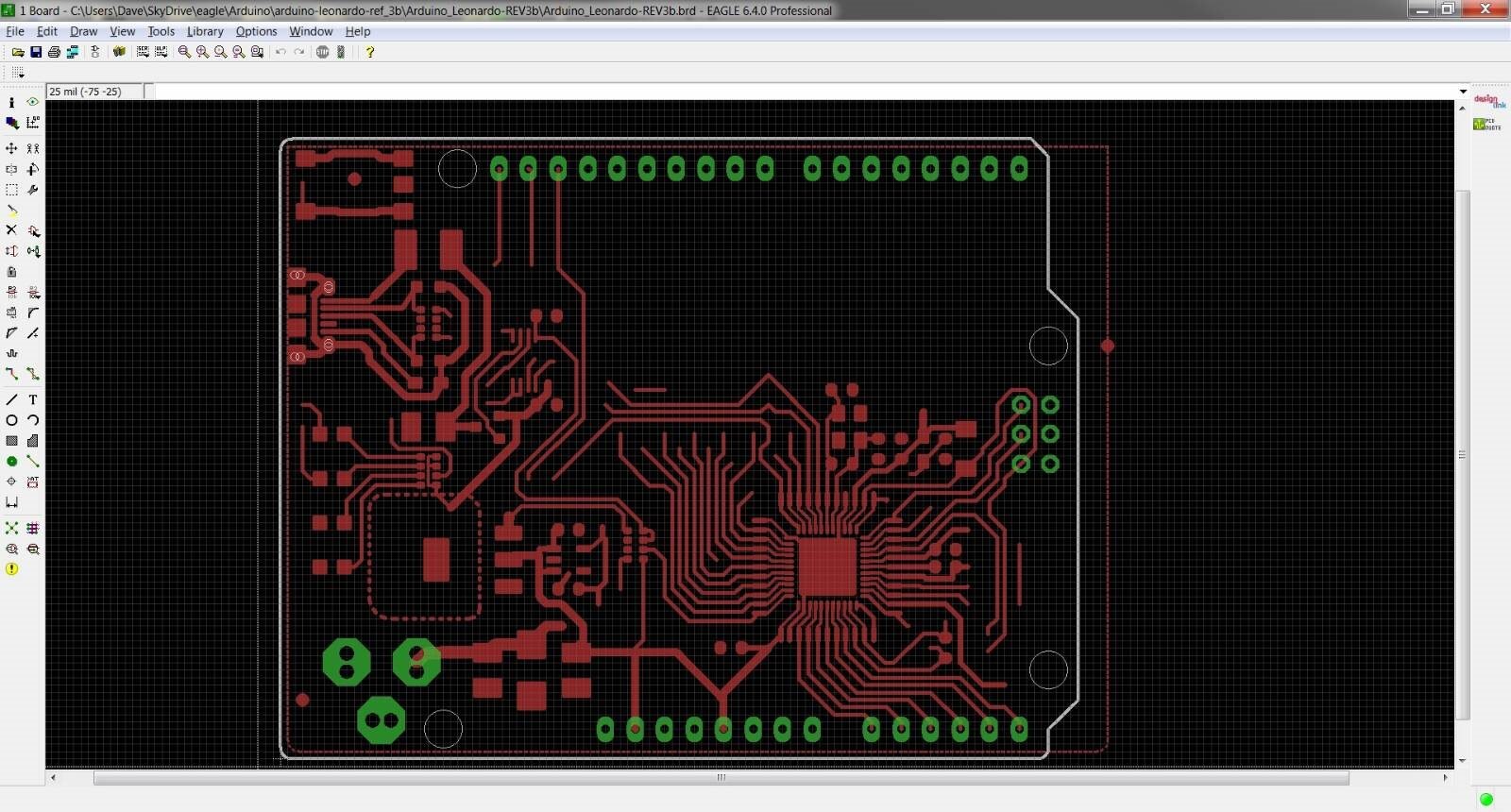
This tutorial is completed with EAGLE v6.4.0, looking at an Arduino Leonardo PCB.


Step 1: With the board file open, select the layers of interest. I like to only look at 'TOP', 'PADS', and 'DIMENSION' layers because this test is only about the copper.


image


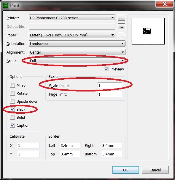
Step 2: Adjust the printer settings for a 1:1 scale, and hit 'Print'. The important settings are highlighted above. Scale factor is obvious, however the area must be 'FULL' since 'WINDOW' will result in an improperly scaled printout. Also, I prefer the 'BLACK' option to be selected since a black-and-white printout will work just fine.

image


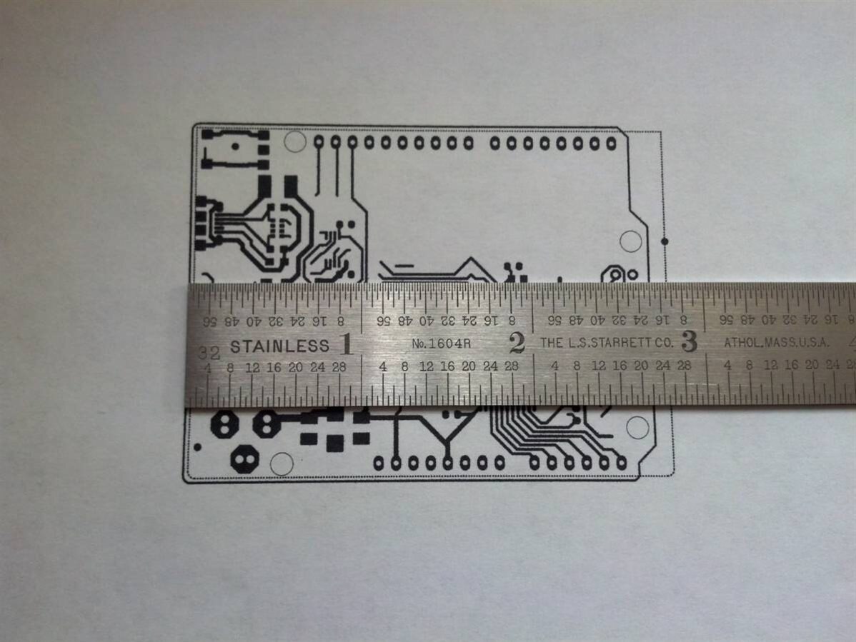
Step 3: Measure the board outline to be positive that all scaling has been done correctly. 


image


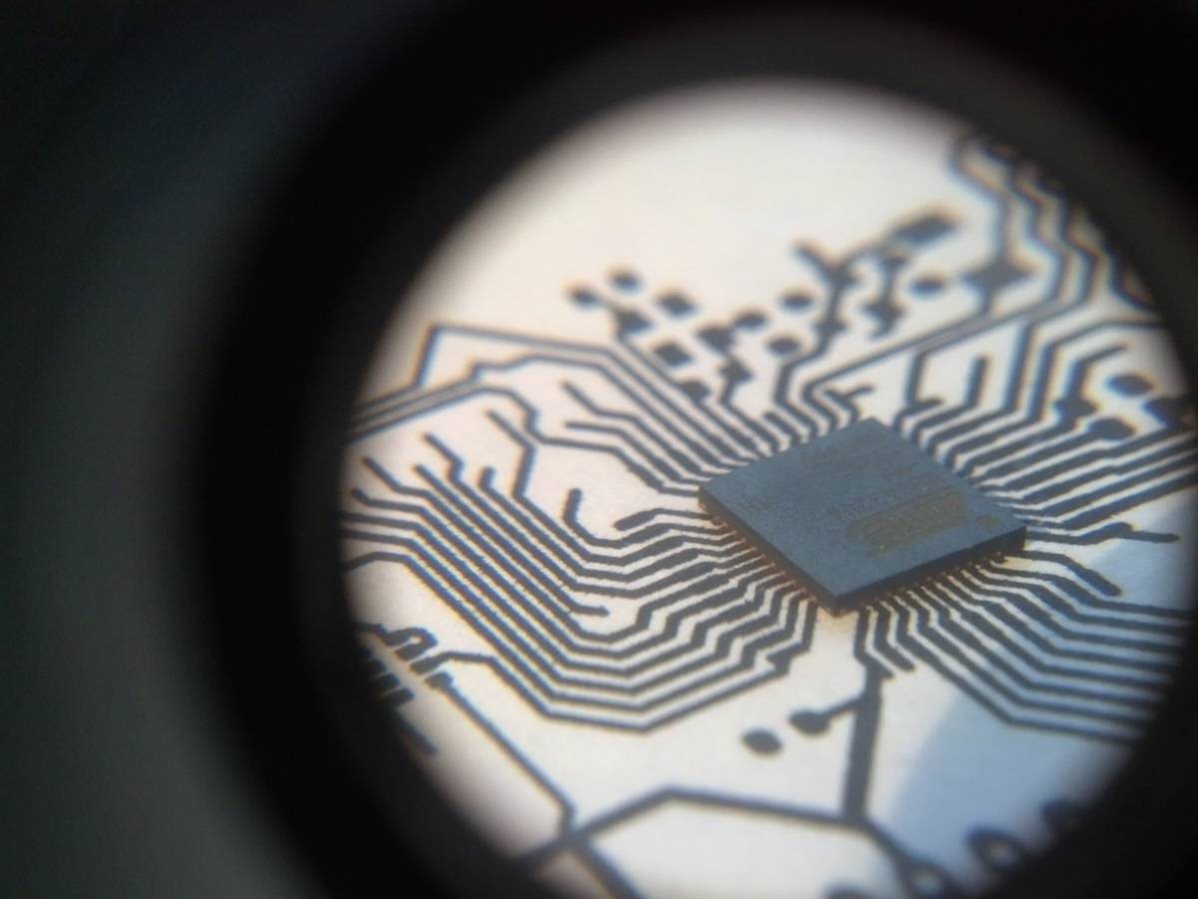
Step 4: Place each component on the printout and verify the footprint is correct. The image above shows a 0.02” pitch 44 QFN placed on a printout from a normal desktop printer. Anything smaller would likely require the use of a laser printer. 

image

Step 5: Repeat steps 1-4 for the components on the bottom side of the PCB.


This technique can also be used when trying to determine the fit in a mechanical enclosure. Gluing the PCB to a piece of cardboard gives the feel of a PCB which can have holes drilled and placed into a mechanical enclosure. One could even go as far as gluing some of the taller components in to check clearances and fit. 


Thanks to the board spins saved, I suggest that this be added to any PCB review. No review is perfect, but this plugs a pretty big hole that exists in normal PCB review steps. Now submit those gerbers with confidence!

  • Sign in to reply
  • Former Member
    Former Member over 10 years ago

    I print my Layout to 200g/m² Paper and cut at the outlines and mounting holes to check if it fits nicely to the planned Case. I had plain wrong datasheets from different manufacturers at several occasions.

    You can even "plug" the paper to headers to check if it fits if you cut a small "x" in every hole. Helped me a lot at the time when there was no good drawing of the RaspberryPi Layout.

    • Cancel
    • Vote Up 0 Vote Down
    • Sign in to reply
    • More
    • Cancel
  • pcosta
    pcosta over 11 years ago

    Yes, it works like a charm. I use this technique for over 20 years and is one of the best ways. also we can use the same paper's PCB outline for checking if the PCB fits correctly in its future place.

    • Cancel
    • Vote Up 0 Vote Down
    • Sign in to reply
    • More
    • Cancel
  • waelect
    waelect over 11 years ago

    Thanks for the blog post, nice and easy method of checking and I will be sure to use it.


    Malcolm

    • Cancel
    • Vote Up 0 Vote Down
    • Sign in to reply
    • More
    • Cancel
  • Richard_H
    Richard_H over 11 years ago

    There is another important option to mention. It is possible to calibrate the printout in x and y direction for the printer. Depending on the printer's qualitiy it might be necessary to adjust this.


    Thanks for your blog.

    Richard

    • Cancel
    • Vote Up 0 Vote Down
    • Sign in to reply
    • More
    • Cancel
element14 Community

element14 is the first online community specifically for engineers. Connect with your peers and get expert answers to your questions.

  • Members
  • Learn
  • Technologies
  • Challenges & Projects
  • Products
  • Store
  • About Us
  • Feedback & Support
  • FAQs
  • Terms of Use
  • Privacy Policy
  • Legal and Copyright Notices
  • Sitemap
  • Cookies

An Avnet Company © 2025 Premier Farnell Limited. All Rights Reserved.

Premier Farnell Ltd, registered in England and Wales (no 00876412), registered office: Farnell House, Forge Lane, Leeds LS12 2NE.

ICP 备案号 10220084.

Follow element14

  • X
  • Facebook
  • linkedin
  • YouTube