element14 Community
element14 Community
    Register Log In
  • Site
  • Search
  • Log In Register
  • About Us
  • Community Hub
    Community Hub
    • What's New on element14
    • Feedback and Support
    • Benefits of Membership
    • Personal Blogs
    • Members Area
    • Achievement Levels
  • Learn
    Learn
    • Ask an Expert
    • eBooks
    • element14 presents
    • Learning Center
    • Tech Spotlight
    • STEM Academy
    • Webinars, Training and Events
    • Learning Groups
  • Technologies
    Technologies
    • 3D Printing
    • FPGA
    • Industrial Automation
    • Internet of Things
    • Power & Energy
    • Sensors
    • Technology Groups
  • Challenges & Projects
    Challenges & Projects
    • Design Challenges
    • element14 presents Projects
    • Project14
    • Arduino Projects
    • Raspberry Pi Projects
    • Project Groups
  • Products
    Products
    • Arduino
    • Avnet Boards Community
    • Dev Tools
    • Manufacturers
    • Multicomp Pro
    • Product Groups
    • Raspberry Pi
    • RoadTests & Reviews
  • Store
    Store
    • Visit Your Store
    • Choose another store...
      • Europe
      •  Austria (German)
      •  Belgium (Dutch, French)
      •  Bulgaria (Bulgarian)
      •  Czech Republic (Czech)
      •  Denmark (Danish)
      •  Estonia (Estonian)
      •  Finland (Finnish)
      •  France (French)
      •  Germany (German)
      •  Hungary (Hungarian)
      •  Ireland
      •  Israel
      •  Italy (Italian)
      •  Latvia (Latvian)
      •  
      •  Lithuania (Lithuanian)
      •  Netherlands (Dutch)
      •  Norway (Norwegian)
      •  Poland (Polish)
      •  Portugal (Portuguese)
      •  Romania (Romanian)
      •  Russia (Russian)
      •  Slovakia (Slovak)
      •  Slovenia (Slovenian)
      •  Spain (Spanish)
      •  Sweden (Swedish)
      •  Switzerland(German, French)
      •  Turkey (Turkish)
      •  United Kingdom
      • Asia Pacific
      •  Australia
      •  China
      •  Hong Kong
      •  India
      •  Korea (Korean)
      •  Malaysia
      •  New Zealand
      •  Philippines
      •  Singapore
      •  Taiwan
      •  Thailand (Thai)
      • Americas
      •  Brazil (Portuguese)
      •  Canada
      •  Mexico (Spanish)
      •  United States
      Can't find the country/region you're looking for? Visit our export site or find a local distributor.
  • Translate
  • Profile
  • Settings
PCB Design, Prototyping and Production
  • Products
  • More
PCB Design, Prototyping and Production
PCB Forum PCB Design for a DC Load
  • Blog
  • Forum
  • Documents
  • Leaderboard
  • Files
  • Members
  • Mentions
  • Sub-Groups
  • Tags
  • More
  • Cancel
  • New
Join PCB Design, Prototyping and Production to participate - click to join for free!
Actions
  • Share
  • More
  • Cancel
Forum Thread Details
  • Replies 17 replies
  • Subscribers 128 subscribers
  • Views 5476 views
  • Users 0 members are here
Related

PCB Design for a DC Load

Andrew J
Andrew J over 3 years ago

cstanton recently posted about PCB manufacturers to see if he could get some action in this forum.  So here goes: this post is in reference to the last PCB I recently designed for an electronic dc load - I didn't find a way to create a blog in this section.  In any case, I've not posted it elsewhere because I wasn't ready to blog about it but it seems like a good candidate to get feedback and comments because:

  1. I've never designed or built something like this before.
  2. It's already designed, manufactured and populated the PCB.  This means that any comments raised can be checked against reality!  So a comment such as "You should check XYZ because I think the ABC will oscillate like a plucked guitar string without a 47K resistor at point HIJ" can be verified.
  3. It's not tested because I haven't yet created the software to drive it.  Any verification will have to wait until l do so.

Unfortunately, if I just posted the PCB it probably wouldn't make much sense, so it requires some explanation and the post is quite long.  This DC load is a module for my Instrument Control Board, thus the driving signals are produced elsewhere and you need to bear that in mind.  

Schematic

Schematic for DC Load Module for the Instrument Control Board

Less-interesting Sub-Sections

Board I/O: incoming power and signals from the ICB.  This module only requires +5V/-5V DC so other power inputs are ignored.  

Temperature Monitors: There were unused ADC outputs so I provisioned space to add two thermocouples which I will attach to the MOSFETS as a back-up temperature monitor, primarily for testing to make sure that my Heatsink Monitor is reasonably accurate and I can judge from differential values when to turn the Fan on/off.

Heatsink Temperature Monitor: There is an I2C driven TO-220 monitor stuck on the heatsink to provide temperature feedback to the ICB which will then drive the fan on/off accordingly.

Indicators: Two LEDs to indicate (a) power is applied to the board (from the IDC); (b) that the DC load is on, i.e. a signal is being received from the ICB and is actively driving current through the MOSFETS.

Fan: connector for a 2-lead fan that will be attached to the case behind the heatsink.

Driving Signals

Choosing a signal to drive the DC Load

The ICB has 4 DAC outputs that could be used.  Nominally, only one is required but I was trying to think about how best to use what is available and I also threw the RTCC_MFP output into the ring.  The latter is a square wave that is generated by the RTCC on the ICB in one of four possible frequencies.  I decided to put a MUX in the signal path so I could choose which output to use: this could be driven from software on the ICB and allow, for example, switching between two output levels or a frequency signal.  DAC C and DAC D are used to control the logic table that 'selects' which input signal appears on the COM pin.  the PWRSIG pin enables/disables the output and is driven from the ICB either through a software switch or a physical momentary button on the ICB enclosure.

DC Load Control

The DC Load control circuitry

This of course is the meat of the DC load module.  I need to be clear up front in that I used a few inputs to create this:

  1. There are a number of posts on E14 that describe a DC Load circuit which I reviewed.  In particular Jan Cumps and Peter (? Sorry, forget the surname now) had a whole set of blog postings on their DC Load design.
  2. John Scully, on YouTube, posted an excelled series on DC Load, in particular parallelsing the MOSFETS for improved outputs.  

The driving signal is coming from the MUX, is buffered and then divided by 10 to give me an input to the driving Op Amp, between 0 and 0.5V.  There's also a trimmer to help with accuracy of this signal.  The signal is then driven into the MOSFETS with feedback to allow 0 to 5A to flow through the MOSFETS - I'll almost certainly limit this to 3A because that is more in line with the PSUs I have and power dissipation I can (economically) achieve.  I do have a PSU that can drive 5A for testing purposes.

I did start off with the MOSFETS in parallel in the most obvious way (not shown, but I'm sure you can picture this setup in your mind.)  The main issue with any approach to paralysing MOSFETS is that they aren't all created equal, so that for, say, any particular Gate Voltage, each MOSFET will allow more current to flow because it has a smaller Rds-ON.  John Scully had experimented with this and fundamentally it came down to these properties of a MOSFET:

RDS-ON as a function of junction temperature Negative temperature co-efficient of Gate-Threshold Voltage

Fig 9 from the datasheet shows that as junction temperature rises, so does Rds-ON.  So in the normal run of things any MOSFET that is driving more current will get hotter thus its Rds-ON will increase and current reduce as a result.  In theory then, there is some self-balancing in the circuit.  However, Figure 7 shows that as junction temperature increases, a lower Gate-Source Threshold is required for the same amount of current.  If the actual GS(th) isn't decreased as temperature increases then it will drive that MOSFET even harder, increasing its temperature with a cyclic feedback on GSth - potentially with thermal runaway for that particular MOSFET.  These two figures really imply that a simplistic approach to parallelising MOSFETS isn't going to work very well at higher currents.  

The circuit shown uses a NPN transistor to bias the GS(th) voltage.  As the voltage over the small resistors (e.g. R12) increases it turns on the transistor which pulls the Gate voltage down thus reducing the GS(th) as temperature increases.  John Scully explains this much better than I can but I'm sure you see the essence of it.  This active feedback helps regulate any MOSFET that would normally want to draw more current than the others.

Sense Feedback

image

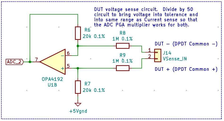
This allows an additional connection from the DUT output terminals to the DC Load Module that provides a more accurate feedback of voltage than that measured directly at the MOSFET outputs which is impacted by lead length, size, components, PCB traces etc.  The choice of resistors reduces the voltage to a level that can be safely input to the ADC 2 channel.  

PCB

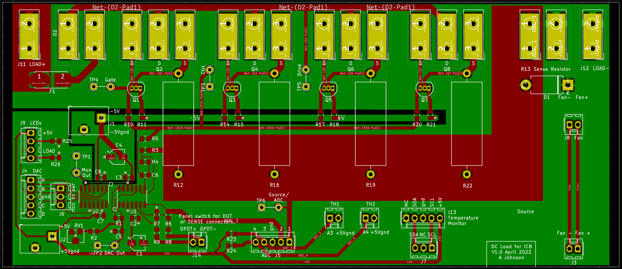
Hopefully the above is enough of an explanation for the PCB to make sense.  It is a 2 layer board, 181mm x 80mm sized to fit the PCB rails in the enclosure I have for it: all signals but one are on the top layer; ground and -5V are on the bottom layer.  The load current path is as large as could be placed whilst maintaining a good clearance to other signals.  All heatsink mounted components wire into the connectors along the top edge.  Other components are placed to ease routing and avoid routing traces onto the bottom layer - successful in all cases except for the COM output of the MUX.

PCB for DC Load

3D view of PCB

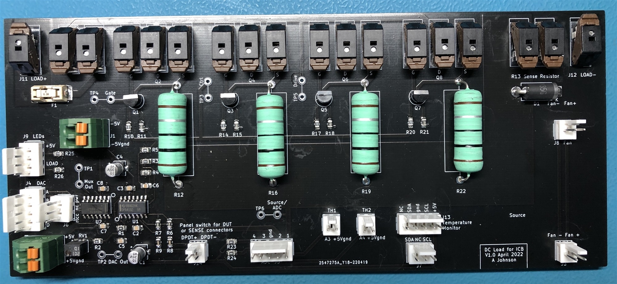
Unfortunately, KICAD doesn't have 3D models for every component but the photo should help:

Photo of populated PCB

As I mentioned at the start, this isn't tested yet as I haven't finished writing the software to drive it from the ICB.  However, please "have at it" and I can report back in the future on any comments made.  As this is meant to be the PCB Prototyping forum, I think it would be useful if any comments were related to real-life experience/problems/successes etc to better help other readers.

  • Sign in to reply
  • Cancel

Top Replies

  • scottiebabe
    scottiebabe over 3 years ago +4
    Most of my comments are personal preference, I'm sure when you power this board up it will function well enough. I really *don't* like your ground net label names, having the ground start with "+5V"…
  • scottiebabe
    scottiebabe over 3 years ago +4
    Another idea you can experiment with is kelvin sensing your current shunt resistor. The resistance of a copper trace with 1oz copper is approximately 0.5 mOhms.sq. You should easily be able to measure…
  • michaelkellett
    michaelkellett over 3 years ago +3
    I'm assuming that Q1 and friends are intended to operate as current limiters in case of short term overload. If so then R11 is the wrong value (typo ?) - 270k is way too big, but 270R would be OK. …
  • cstanton
    cstanton over 3 years ago
    Andrew J said:
    I didn't find a way to create a blog in this section.

    Fixed Smiley Thanks for posting!

    And something weird's going on with the images there, they're so wide they're being cut off, I'll check that up with the dev' team, until then you might want to click on them and edit their width/height. Slight smile

    • Cancel
    • Vote Up +1 Vote Down
    • Sign in to reply
    • Cancel
  • Andrew J
    Andrew J over 3 years ago in reply to cstanton

    When I click on them, I get the full size.  If I edit them to reduce the size, I presume that is purely within the posting?

    • Cancel
    • Vote Up 0 Vote Down
    • Sign in to reply
    • Cancel
  • Andrew J
    Andrew J over 3 years ago in reply to Andrew J

    Yes, it is!!

    • Cancel
    • Vote Up +1 Vote Down
    • Sign in to reply
    • Cancel
  • shabaz
    shabaz over 3 years ago

    Hi Andrew,

    Very nice board, it looks well laid out, I've never built a DC load but it looks pretty reasonable to me. I was wondering, are the large resistors required to be 1 ohm, or was that a placeholder value? I was wondering if much lower resistances could be used, especially if all MOSFETs are going to the same heatsink.

    It's a challenge to have a short path through the DC load when it has to go through physically large components, I too had this issue, and I'm not sure mine is a good solution, but I'll paste it here in case it gives any ideas for your board, or if mine has glaring errors in it too! My boards have arrived, so it is what it is for my prototype too. Mine was a MOSFET testbed, not a DC load, and was easier since I didn't have 4 MOSFETs to battle with. I used screw stud-type terminals, I think I would use connectors if I could go back in time. Also, my board is 4-layer since it is small compared to yours, and therefore the cost difference was small. I didn't use all 4 layers fully much, but was slightly handy for the high current path, and creating a bit of a shield for induced signals.

    image

    Some ideas to rule in/out for your future PCB could be as follows (these are all really minor, and not necessarily better, they are just a bouncing of ideas between engineers : )  

    (1) Maybe use SMA connectors for test points related to MOSFET signals, gate voltage, etc., the connectors are cheap from (say) LCSC, it's not affordable to buy them from Farnell unless you need high quality ones for RF purposes. For test signals, any cheap SMA connectors would be fine. They can then be directly screwed into your 'scope via SMA cables and SMA-to-BNC adapters. Maybe not essential, but if you have the SMA footprints, they can be left unsoldered and used as testpoints anyway as well.

    (2) Holes for mounting, granted you may be using a slide-in case that doesn't require it!

    (3) The default TO-92 BJT footprint holes in KiCAD are in-line, which is more awkward to solder, they could be replaced with the triangle layout.

    (4) Maybe worth considering to consolidate the connectors to one or two flat flex cables for the processor connections etc, they are probably cheaper than normal sockets/plugs, and less effort than making up crimped cables. It is also easy to solder wires to 1mm pitch footprints, so if worst case you needed to make some unplanned connections for your prototype, then you could omit soldering the flat flex connector and just patching wires to it (or have FFC and 0.1 inch header pins on the board).

    (5) I can't tell, are the connectors on your board for directly mounting MOSFETs? If so, are they on round millimetre offsets? Otherwise, it's a pain to drill out a heatsink. When placing off-board parts, or external connectors or controls etc., I've found it convenient to place them on a millimetre grid rather than imperial mil etc.

    Anyway, the DC load is an interesting project and a great-looking board from my perspective, and looking forward to hearing how it goes : )

    • Cancel
    • Vote Up +2 Vote Down
    • Sign in to reply
    • Cancel
  • michaelkellett
    michaelkellett over 3 years ago

    I'm assuming that Q1 and friends are intended to operate as current limiters in case of short term overload.

    If so then R11 is the wrong value (typo ?)  - 270k is way too big, but 270R would be OK.

    I would normally put a resistor in the base ciruit of Q1 and no resistor in the emitter circuit. You need one or the other (or both) so that Q1 doesn't try to clamp the voltage across R12 with its base/emitter junction.

    Your cicruit will suffer from a common problem with DC loads (including mid priced commercial ones.).

    If you set it as a current sink with a non zero current and no applied voltage at J11  then U1c will saturate with maximum positive output. All the power MOSFETs will be turned on and their gates fully charged up.

    When voltage is applied the initial current spike will be huge. It will go on for some time because the MOSFET drive resistors are so big and because of the10us time constant of C6/R3.

    I have a Rigol load which has a similar issue, it is not possible to get an Infineon protected high side switch to apply 24V to the load (set for 1A) because the initial current spike trips the 20A hard limit on the high side switch. I found this to my cost when I designed a multichannel test rig that used the Rigol load for measuring Disappointed

    I've spent some time trying to think round this issue, so far without much success.

    You may be able to mitigate it in software.

    MK

    • Cancel
    • Vote Up +3 Vote Down
    • Sign in to reply
    • Cancel
  • Andrew J
    Andrew J over 3 years ago in reply to shabaz

    Thanks Shabaz.

    Using 0.1Ohm resistors was a start point in dealing with the slight construction differences in the parallel MOSFETS to help balance out the negative Vgsth co-efficient - any MOSFET that was drawing slightly more current would cause a larger voltage drop over the resistor, thus reducing Vgs and the current draw.  In practice, in conjunction with the NPN transistors which provide the active feedback, it seemed to work better with a higher value - 1 ohm - without the (potential) drawback that it has a bigger impact on the circuit because it causes an even bigger voltage drop. I’m benefiting here from the results of experimentation! 

    I want to be clear here, again, that I owe John Scully a lot for this parallelisation circuit and real-world observation.  I started off with a bog standard parallel design but from research it was clear that would cause issues, particularly at higher currents.

    All the MOSFETS will be mounted on an off-board heatsink and I wanted an easy way to connect them to the board without having to provide soldering holes and then carefully position the PCB/heatsink together to not strain them.  That would of course have the benefit of shorter paths.  My start point is that the active feedback to balance the MOSFETS and short wires from the MOSFET to the board connectors won't have a big impact, or nothing that can't be adjusted from the readings in the Sense circuit - something to look at though.  The connectors I've plumped for are these: Metz Connect spring loaded connectors

    The other connectors are ones I had to hand which is why they are a mix.  It's interesting you mention ribbon cable because I did start off with that premise.  However, as I was laying out the board it became much easier to stick to two layers with signals on the top layer if I could distribute the board connectors over the surface - hence why they're sort of all over the place!

    The biggest issue I had with connectors, in general, were finding ones that were mountable on a panel.  

    (1) I'll check out SMA connectors on my next board.  I went with what I have/used to without giving it much consideration TBH.  It's a good idea.

    (2) Very specifically this time I designed the PCB in conjunction with an enclosure - in this case, one that has rails to slot a PCB into, hence the 181mm wide board.  I normally add mounting holes of 3.2mm diameter for an M3 mount.  Pretty much every single time I've built up a PCB, looked for a case only to find if I'd done that first I may have a wider and cheaper choice.  It's also very hard to filter enclosures on retailer websites as they don't seem to use height/width/depth consistently.

    (3) Yeh, they were a pain to solder you're right, and I did have to rework one of them.  Worse, I've been bitten before.

    (5) The MOSFETS are all heatsink mountable and I don't know if the spacing of the connector footprint would actually allow them to be soldered to the board.  I think I understand your point though - I have seen instances of MOSFETS soldered to the board then attached to the heatsink and I considered that to be difficult to do accurately.  Seems from your experience I was right.

    • Cancel
    • Vote Up +1 Vote Down
    • Sign in to reply
    • Cancel
  • Andrew J
    Andrew J over 3 years ago in reply to michaelkellett

    Thanks Michael.

    The NPN transistors (Q1 and friends) are a form of current limiting in the sense they are part of an active feedback for a MOSFET that would want to normally draw more current because of its’ construction difference.  They are used to drag down the voltage on the gate (Vgs) to reduce the current through the MOSFET to help keep them in balance. This is all part of dealing with a Rds-on positive temperature impact and a Vgsth negative temperature impact.  It started with a lower valued emitter resistor but changed to 270K as a result of increasing the Source resistor, e.g. R12, to 1Ohm.

    As I mention above, I've benefitted a lot from John Scully's work on this particular aspect and his real-life observations.     

    The switch on surge is interesting observation and I'll have to watch out for that.  The DAC in the ICB starts up at 0V output, though in theory it can be configured alternately, and the MUX output is also off because the PWRSIG input is low.  So at startup there should be no issue with a non-zero current at U1C, but one to watch out for - I mention it because some DACs power up at midpoint by default.  Dealing with a non-zero current and no voltage after startup, I might be able to handle differently.  To apply current, PWRSIG has to go high: even though there is a physical button and a touch button to do this, it is still software driven.  If through the Sense circuit (which is active even if no sense cables are plugged in) I read zero volts I could prevent PWRSIG from being raised.

    I suppose the big question there is: in testing that, is anything likely to blow?  I've tried to put in a fair bit of protection to prevent damage to expensive components but it would be good to understand the risk.

    • Cancel
    • Vote Up +1 Vote Down
    • Sign in to reply
    • Cancel
  • jc2048
    jc2048 over 3 years ago

    These are a few random thoughts, in random order, from a quick view of the board.

    I can't see where -5Vgnd joins +5Vgnd. Does that happen off the board? As it stands, -5V doesn't seem like it would have any relationship to the other voltages on the board.

    Some of the high current tracking could be a more generous. The track from pin 2 of the fuse to the connector, and the track across the top, 'Net-(D2-Pad1)', in particular. The track you've got is about the minimum you need for 5A (assuming a 20C rise, which is the kind of conservative figure you'd go with for something commercial), but you've got room to make it much better than that.

    What kind of 1R resistors are they? Are they wirewound? Inductance? Temperature coefficient?

    The transistor footprint looks horrible.

    I can't get my head round whether the transistor feedback does what you want or not. Is it possible that it works simply by virtue of the added resistors (in the same way that adding emitter resistors allows BJTs to be paralleled)?

    What's the contact resistance of the non-screw terminals? I'd be a bit nervous of using something like that to wire power devices to a pcb. Maybe that's just prejudice and being very old-fashioned on my part.

    It feels to me like you're building too much inductance into the high-current output loop, both with the layout (separating load+ and load-, and so forcing the external wiring to be a wide loop to follow suit) and having all these loops off the board to the various power devices, but maybe it will be ok. We'll find out when you try it. 

    • Cancel
    • Vote Up +3 Vote Down
    • Sign in to reply
    • Cancel
  • Andrew J
    Andrew J over 3 years ago in reply to jc2048

    Thanks John.  

    I take note of your comments on layout and trace sizes.  It will be interesting to see how it tests out when I get around to it  If this causes issues, I think I'd go back to the drawing board and relayout those connections and design them to either direct mount the MOSFETs on the board or re-arrange the solder points to allow direct solder wire rather than use connectors.

    This is a module for my ICB so is designed to be driven by that: all grounds are tied at one point there.

    The 1R resistors are wire-wound: Buy Now .  The connectors are rated to 300V 9A and can take quite a thick wire (up to 16AWG) so should be ok - there's no information on contact resistance though, which I hadn't thought about until you mentioned it!  Datasheet link in a post above.

    I'm not sure what you mean by the transistor footprint looks horrible - you mean aesthetically? Functionally?

    • Cancel
    • Vote Up +2 Vote Down
    • Sign in to reply
    • Cancel
  • jc2048
    jc2048 over 3 years ago in reply to Andrew J

    Personally, I'd common the grounds on the board, not back at the power supply. If this was a commercial product, you'd filter the power coming on to the board, so you want the common point to be the plane immediately after that (and rely on the low inductance and low resistance of the plane to make that the same, as far as possible, over the whole extent of the board). Otherwise you've got the lead inductance and the filters between different points of what you would hope would be a common reference ground.

    Two things to think about with the resistors.

    A wirewound resistor is a coil of wire that has a dc resistance of the chosen value (in this case 1R). But coils also have inductance, so at a megahertz it's going to be behaving somewhat differently to a pure resistor. Although you've slugged the op amp, so that it doesn't get too frisky above a few tens of kilohertz, the MOSFET and the BJT can probably manage a bit of mischievous behaviour up there AND you've got that gate capacitance that will happily resonate with an inductance if there's a bit of gain to keep everything going. I'm not saying that it will be a problem at all, just that it's an 'amber light' so to speak - something to be aware of and to look at.

    The temp coefficient might be as bad as 400ppm/C (according to the datasheet). That's approx 0.4mR/C for a 1R resistor. The temperature rise for 20% of the rated wattage is about 20C (graph on datasheet), so your resistance change from 0 to full current might be 8mR, or so. How does that sit with what your sharing circuit is doing? Not necessarily a problem - might even help you, but again worth a look.

    Better resistors are available for power work. Thick film resistors have better temperature specs and can be much lower in inductance.

    The connectors might be ok. If they can carry 9A then the contact resistance can't be too high. But with 2 for the diode, 2 for the MOSFET, and 2 for the sense resistor in the high current path, that's getting to be a fair amount of extra resistance.

    Don't mind me over the transistor. I'm just old. The TO92 package replaced metal can parts that had the middle pin offset to give a triangle shape to the arrangement. So the TO92 parts would have the pins formed to the same pattern (you could even buy them ready formed). There were plastic supports that you could buy that would form the leads and support the transistor above the board. The reason for the support, though, was more than just shaping the legs. If you have a package like that and solder it hard against a board, which you can do with the footprint you've got, then temperature cycling of the whole thing can damage the transistor - the support acts as a buffer between the two.

    • Cancel
    • Vote Up +3 Vote Down
    • Sign in to reply
    • Cancel
>
element14 Community

element14 is the first online community specifically for engineers. Connect with your peers and get expert answers to your questions.

  • Members
  • Learn
  • Technologies
  • Challenges & Projects
  • Products
  • Store
  • About Us
  • Feedback & Support
  • FAQs
  • Terms of Use
  • Privacy Policy
  • Legal and Copyright Notices
  • Sitemap
  • Cookies

An Avnet Company © 2025 Premier Farnell Limited. All Rights Reserved.

Premier Farnell Ltd, registered in England and Wales (no 00876412), registered office: Farnell House, Forge Lane, Leeds LS12 2NE.

ICP 备案号 10220084.

Follow element14

  • X
  • Facebook
  • linkedin
  • YouTube