element14 Community
element14 Community
    Register Log In
  • Site
  • Search
  • Log In Register
  • Community Hub
    Community Hub
    • What's New on element14
    • Feedback and Support
    • Benefits of Membership
    • Personal Blogs
    • Members Area
    • Achievement Levels
  • Learn
    Learn
    • Ask an Expert
    • eBooks
    • element14 presents
    • Learning Center
    • Tech Spotlight
    • STEM Academy
    • Webinars, Training and Events
    • Learning Groups
  • Technologies
    Technologies
    • 3D Printing
    • FPGA
    • Industrial Automation
    • Internet of Things
    • Power & Energy
    • Sensors
    • Technology Groups
  • Challenges & Projects
    Challenges & Projects
    • Design Challenges
    • element14 presents Projects
    • Project14
    • Arduino Projects
    • Raspberry Pi Projects
    • Project Groups
  • Products
    Products
    • Arduino
    • Avnet Boards Community
    • Dev Tools
    • Manufacturers
    • Multicomp Pro
    • Product Groups
    • Raspberry Pi
    • RoadTests & Reviews
  • About Us
  • Store
    Store
    • Visit Your Store
    • Choose another store...
      • Europe
      •  Austria (German)
      •  Belgium (Dutch, French)
      •  Bulgaria (Bulgarian)
      •  Czech Republic (Czech)
      •  Denmark (Danish)
      •  Estonia (Estonian)
      •  Finland (Finnish)
      •  France (French)
      •  Germany (German)
      •  Hungary (Hungarian)
      •  Ireland
      •  Israel
      •  Italy (Italian)
      •  Latvia (Latvian)
      •  
      •  Lithuania (Lithuanian)
      •  Netherlands (Dutch)
      •  Norway (Norwegian)
      •  Poland (Polish)
      •  Portugal (Portuguese)
      •  Romania (Romanian)
      •  Russia (Russian)
      •  Slovakia (Slovak)
      •  Slovenia (Slovenian)
      •  Spain (Spanish)
      •  Sweden (Swedish)
      •  Switzerland(German, French)
      •  Turkey (Turkish)
      •  United Kingdom
      • Asia Pacific
      •  Australia
      •  China
      •  Hong Kong
      •  India
      •  Korea (Korean)
      •  Malaysia
      •  New Zealand
      •  Philippines
      •  Singapore
      •  Taiwan
      •  Thailand (Thai)
      • Americas
      •  Brazil (Portuguese)
      •  Canada
      •  Mexico (Spanish)
      •  United States
      Can't find the country/region you're looking for? Visit our export site or find a local distributor.
  • Translate
  • Profile
  • Settings
PCB Design, Prototyping and Production
  • Products
  • More
PCB Design, Prototyping and Production
PCB Forum Symbols and footprint support for Arduino in KiCad 7.x
  • Blog
  • Forum
  • Documents
  • Leaderboard
  • Files
  • Members
  • Mentions
  • Sub-Groups
  • Tags
  • More
  • Cancel
  • New
Join PCB Design, Prototyping and Production to participate - click to join for free!
Actions
  • Share
  • More
  • Cancel
Forum Thread Details
  • Replies 13 replies
  • Subscribers 124 subscribers
  • Views 7361 views
  • Users 0 members are here
  • arduino kicad
  • arduino libraries
Related

Symbols and footprint support for Arduino in KiCad 7.x

colporteur
colporteur over 2 years ago

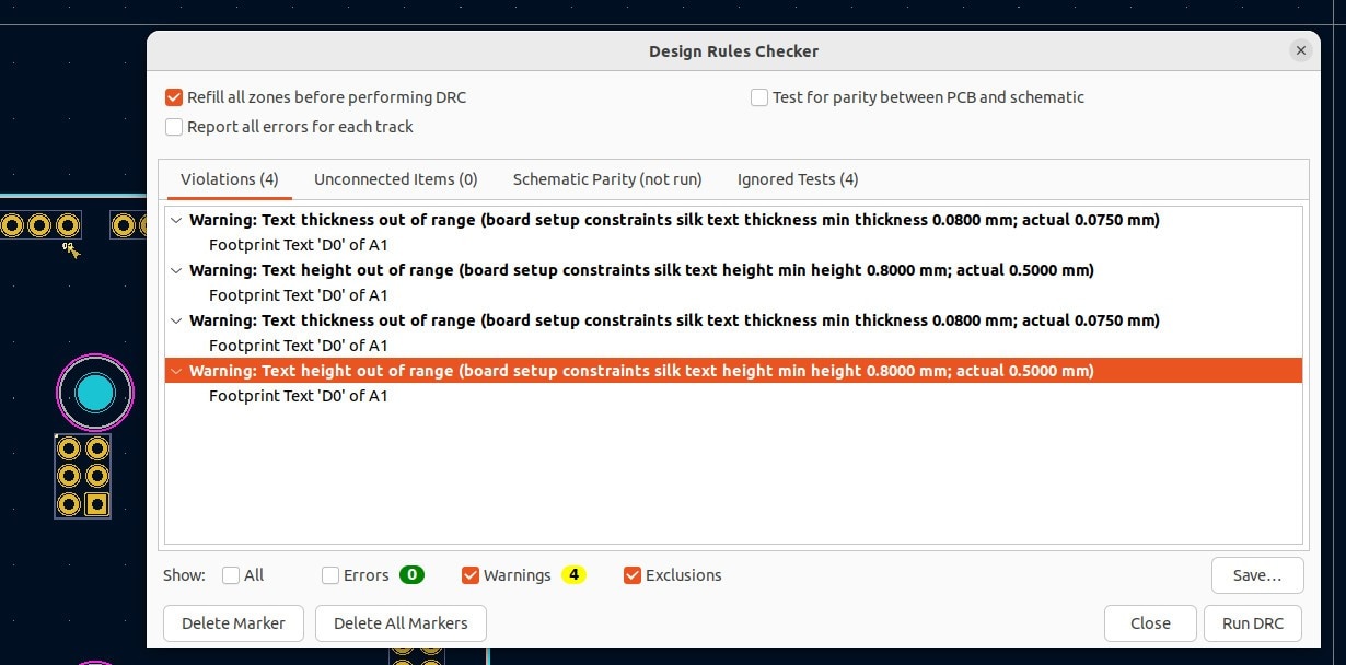
I've encountered some Design Rules Checker warning messages when creating a PCB, that appear to be related to the libraries provided at https://github.com/Alarm-Siren/arduino-kicad-library . I'm wondering if members have any experience using the libraries provided at this link.

image

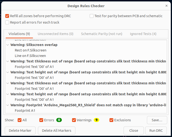
The libraries appear to be the official support for the Arduino. I used the Arduino_Mega2560_R3_shield footprint on a test PCB without adding any components and received the same warnings.

image

This is the first time I have used these libraries. I followed the install instructions at the site and also tried installing the libraries manually. I get the warning no matter how they are installed. I noticed some anomalies when I looked closer at the templates. The lines highlight some of them. (i.e. there are a few orphaned D0's). These appear to be what DRC is complaining about.

Since I haven't used these libraries before I curious if anyone can share their experience.

  • Sign in to reply
  • Cancel

Top Replies

  • shabaz
    shabaz over 2 years ago +6
    Hi Sean, They are just warnings so they are unlikely to cause harm, having said that, as you say, it looks like it is related to that text etc. The library is just created by an individual, not an…
  • colporteur
    colporteur over 2 years ago in reply to alarmsiren +2
    Thank you for the reply. My intention in making the post was to rule out PBKECK, problem between keyboard and chair. I am new to KiCAD 7 and KiCAD in general. There was a very strong likelihood the problem…
  • alarmsiren
    alarmsiren over 2 years ago +1
    Hi Colporteur, I am the creator of this library, and I'm sorry that you have had trouble with it. From what I can see, some of your warnings are unrelated to the library - the only four I can replicate…
Parents
  • alarmsiren
    alarmsiren over 2 years ago

    Hi Colporteur,

    I am the creator of this library, and I'm sorry that you have had trouble with it.

    From what I can see, some of your warnings are unrelated to the library - the only four I can replicate are the Text Thickness warnings. These are not errors per se, the minimum silkscreen thickness is configurable in the DRC settings. It just so happens that the default minimum silkscreen thickness in the DRC settings in Kicad 7 is larger than I use in the library. This is something that I missed in my testing and I apologise: I have raised a bug and will endeavour to fix this in the next release of the library (see: https://github.com/Alarm-Siren/arduino-kicad-library/issues/93). However, as a temporary measure, it is very easy for you to fix yourself - you can update the label's text thickness, or you can change the DRC settings so it won't complain. Alternatively, you can safely ignore these warnings if you prefer.

    Though I don't know why they are in the positions they are - perhaps you moved them? - the D0s are deliberate and are originally placed to mark the 'D0' pin on the footprint, for orientation and troubleshooting purposes. There is no reason why these would generate any warnings (beyond the text thickness issue already mentioned), and do not do so in my testing.

    As to the replacement of the symbol with an updated version that moved the voltage pins around, I'm sorry that this caused you some consternation. However, this was an improvement applied to all the symbols in version 3.0.0 back in Feburary, and clearly documented in the release notes for that version (see: https://github.com/Alarm-Siren/arduino-kicad-library/releases/tag/v3.0.0). Additionally, the library uses semantic versioning such that when the major number increments (e.g. from v2.x.x to v3.x.x, as happened in this case) this is a signal to the user that breaking changes have been implemented.

    For the future, if you're having a problem with someone's library on GitHub, the best place to get help is in the bug tracker of the library itself (in this case of this library, here: https://github.com/Alarm-Siren/arduino-kicad-library/issues), as mentioned in the README file. Posting about the problem in a totally unrelated forum, which I only came across by pure chance, and being quite rude about something I work very hard to maintain for free, is not helpful either for you or for me. I'm only human, and I make mistakes as everyone does, but if people don't tell me about those mistakes how am I supposed to fix them?

    As Shabaz said, and for the avoidance of doubt, no the library is not created by nor affiliated with Arduino in any way (as stated in the README file), and the library is provided as-is without any warranty of any kind - you use it at your own risk. That being said, aside from the occassional niggle, I am confident in the quality of my work: I've personally used many of the footprints in my own designs without issue, and all of them are verified against official Arduino documentation. I do all of this, for free, to give back to the community, because I feel like being helpful.

    • Cancel
    • Vote Up +1 Vote Down
    • Sign in to reply
    • Cancel
  • colporteur
    colporteur over 2 years ago in reply to alarmsiren

    Thank you for the reply. My intention in making the post was to rule out PBKECK, problem between keyboard and chair. I am new to KiCAD 7 and KiCAD in general. There was a very strong likelihood the problem originate with me.

    If my comments were perceived as criticism I would like to change the perception. I sense a defensiveness in your response.  I reap the benefit of the riches when people share. I'm cognitive of the altruism in volunteering to contribute. It is a gift, accepted with appreciation. Hopefully to be never taken for granted.

    Perhaps I've moved something...that is possible lacking experience so I tried it a few times. I've used the mega template again and the errant D0 was still there. I captured the screen shot again. If the lone D0 is by design for orientation than I have learned something.

    image

    I disagree with your position on where the appropriate place was to make a post.  The post was me merely was trying to determine if it was something I did or didn't do within a community that is safe and comments are respected. You have perceived something in my post that you take personally. Your knowledge made this a niggle. My knowledge with four warnings I had never received before make it a concern, I wished to investigate.

    My post was never a personal attack on the content. If I was confident and I fully understood the issue, I would provide feedback that could correct it., I may have posted to GITHUB. 

    • Cancel
    • Vote Up +2 Vote Down
    • Sign in to reply
    • Cancel
  • alarmsiren
    alarmsiren over 2 years ago in reply to colporteur

    I accept your explanation, and I apologise for over-reacting. In hindsight I can see that the parts which made me angry (and I was angry - though I did my best to tone that down in the actual reply) were more general expressions of frustration than direct attacks on the library or me.

    Back to the matter at hand, the D0s themselves are not errant, they are supposed to be there. My reference to them being moved is because in your original screenshot they are not where they ought to be; in your new screenshot I can see that they are so that's fine.

    The warnings you are receiving can be safely ignored, but if you want to make them go away you can adjust the DRC settings for your layout. The relevant settings can be found in File -> Board Setup -> Design Rules -> Constraints; then set Minimum Text Height to 0.5mm and Minimum Text Thickness to 0.075mm. Of course, this is assuming that your PCB fabricator is capable of creating silkscreen of this size - DRC is meaningless if you don't input the desired settings (usually those provided by the PCB fab you intend to use).

    Nevertheless, I do want my library to work without problems/warnings for the 'default' configuration - its supposed to be as novice friendly as I can make it - so I will be changing text height and thickness of the affected silkscreen elements in the next update of the library.

    In my defense, these silkscreen DRC checks are a new feature in Kicad 7 and I do most of my testing in Kicad 6, so I simply hadn't come across this problem yet.

    • Cancel
    • Vote Up 0 Vote Down
    • Sign in to reply
    • Cancel
  • shabaz
    shabaz over 2 years ago in reply to alarmsiren

    Regarding silkscreen, in case it helps here are some values I'm using. I used to use quite small labels and thin lines, but have moved to larger/thicker where possible because often people will struggle with the smallest sizes without glasses/magnifiers etc. The screenshot below shows what I'm currently aiming at, although it's not always possible. I've gone for 0.15 mm line thickness minimum (some older footprints that I use have thinner lines currently : ( and for the text I'll go for a large size but scale it down a bit if it cannot fit. For example, the text on the left side is the same height as the text on the right side, but I squashed it horizontally a bit, in the belief that keeping the height could be beneficial even if the text looks squashed. I have no idea if that's good or not, I'll find out soon when the board is made!

    image

    • Cancel
    • Vote Up 0 Vote Down
    • Sign in to reply
    • Cancel
Reply
  • shabaz
    shabaz over 2 years ago in reply to alarmsiren

    Regarding silkscreen, in case it helps here are some values I'm using. I used to use quite small labels and thin lines, but have moved to larger/thicker where possible because often people will struggle with the smallest sizes without glasses/magnifiers etc. The screenshot below shows what I'm currently aiming at, although it's not always possible. I've gone for 0.15 mm line thickness minimum (some older footprints that I use have thinner lines currently : ( and for the text I'll go for a large size but scale it down a bit if it cannot fit. For example, the text on the left side is the same height as the text on the right side, but I squashed it horizontally a bit, in the belief that keeping the height could be beneficial even if the text looks squashed. I have no idea if that's good or not, I'll find out soon when the board is made!

    image

    • Cancel
    • Vote Up 0 Vote Down
    • Sign in to reply
    • Cancel
Children
  • alarmsiren
    alarmsiren over 2 years ago in reply to shabaz

    Thanks for the suggestions. The Kicad Library Conventions (https://klc.kicad.org/#f5) recommend a height and width of 1mm, thickness 0.15mm for text. As I have a long-term intention to bring the library into compliance with the KLC, I will be using these values.

    • Cancel
    • Vote Up 0 Vote Down
    • Sign in to reply
    • Cancel
element14 Community

element14 is the first online community specifically for engineers. Connect with your peers and get expert answers to your questions.

  • Members
  • Learn
  • Technologies
  • Challenges & Projects
  • Products
  • Store
  • About Us
  • Feedback & Support
  • FAQs
  • Terms of Use
  • Privacy Policy
  • Legal and Copyright Notices
  • Sitemap
  • Cookies

An Avnet Company © 2025 Premier Farnell Limited. All Rights Reserved.

Premier Farnell Ltd, registered in England and Wales (no 00876412), registered office: Farnell House, Forge Lane, Leeds LS12 2NE.

ICP 备案号 10220084.

Follow element14

  • X
  • Facebook
  • linkedin
  • YouTube