element14 Community
element14 Community
    Register Log In
  • Site
  • Search
  • Log In Register
  • About Us
  • Community Hub
    Community Hub
    • What's New on element14
    • Feedback and Support
    • Benefits of Membership
    • Personal Blogs
    • Members Area
    • Achievement Levels
  • Learn
    Learn
    • Ask an Expert
    • eBooks
    • element14 presents
    • Learning Center
    • Tech Spotlight
    • STEM Academy
    • Webinars, Training and Events
    • Learning Groups
  • Technologies
    Technologies
    • 3D Printing
    • FPGA
    • Industrial Automation
    • Internet of Things
    • Power & Energy
    • Sensors
    • Technology Groups
  • Challenges & Projects
    Challenges & Projects
    • Design Challenges
    • element14 presents Projects
    • Project14
    • Arduino Projects
    • Raspberry Pi Projects
    • Project Groups
  • Products
    Products
    • Arduino
    • Avnet Boards Community
    • Dev Tools
    • Manufacturers
    • Multicomp Pro
    • Product Groups
    • Raspberry Pi
    • RoadTests & Reviews
  • Store
    Store
    • Visit Your Store
    • Choose another store...
      • Europe
      •  Austria (German)
      •  Belgium (Dutch, French)
      •  Bulgaria (Bulgarian)
      •  Czech Republic (Czech)
      •  Denmark (Danish)
      •  Estonia (Estonian)
      •  Finland (Finnish)
      •  France (French)
      •  Germany (German)
      •  Hungary (Hungarian)
      •  Ireland
      •  Israel
      •  Italy (Italian)
      •  Latvia (Latvian)
      •  
      •  Lithuania (Lithuanian)
      •  Netherlands (Dutch)
      •  Norway (Norwegian)
      •  Poland (Polish)
      •  Portugal (Portuguese)
      •  Romania (Romanian)
      •  Russia (Russian)
      •  Slovakia (Slovak)
      •  Slovenia (Slovenian)
      •  Spain (Spanish)
      •  Sweden (Swedish)
      •  Switzerland(German, French)
      •  Turkey (Turkish)
      •  United Kingdom
      • Asia Pacific
      •  Australia
      •  China
      •  Hong Kong
      •  India
      •  Korea (Korean)
      •  Malaysia
      •  New Zealand
      •  Philippines
      •  Singapore
      •  Taiwan
      •  Thailand (Thai)
      • Americas
      •  Brazil (Portuguese)
      •  Canada
      •  Mexico (Spanish)
      •  United States
      Can't find the country/region you're looking for? Visit our export site or find a local distributor.
  • Translate
  • Profile
  • Settings
PCB Design, Prototyping and Production
  • Products
  • More
PCB Design, Prototyping and Production
PCB Forum DIP Package Inductance Simulation
  • Blog
  • Forum
  • Documents
  • Leaderboard
  • Files
  • Members
  • Mentions
  • Sub-Groups
  • Tags
  • More
  • Cancel
  • New
Join PCB Design, Prototyping and Production to participate - click to join for free!
Actions
  • Share
  • More
  • Cancel
Forum Thread Details
  • Replies 7 replies
  • Subscribers 124 subscribers
  • Views 1257 views
  • Users 0 members are here
Related

DIP Package Inductance Simulation

scottiebabe
scottiebabe over 1 year ago

image

The sun has long set on Dual inline Packages (DIP) for high speed digital components. I have joked the Advanced High-speed CMOS (AHC) family in the 74 series are too fast for their own good in a DIP package. 

The industry standard pinout of the 74x logic series puts the power supply connections at opposing corners of the IC; namely pins 7 and 14. This results in the longest package interconnect path for IC to PCB landing pads and consequently more opportunities for RLC parasitics to creep into the PDN network from the perspective of silicon die.

What does the literature have to say?

A TI application note: AN-1205 Electrical Performance of Packages (https://www.ti.com/lit/an/snoa405a/snoa405a.pdf)

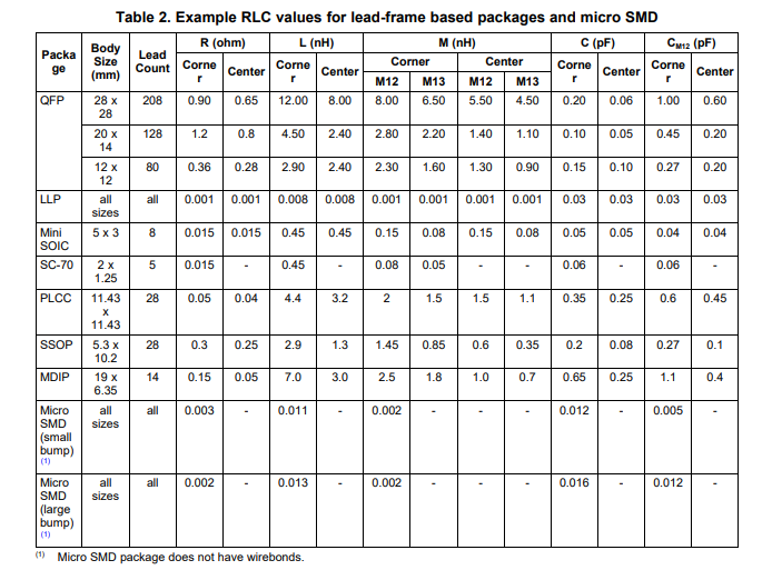
Claims a DIP-14 package has approximately 7 nH of interconnect inductance for the corner leads.

image

Simulation

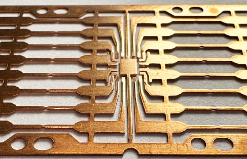
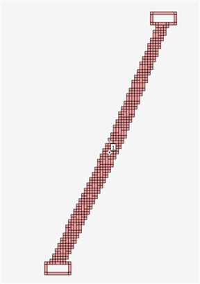
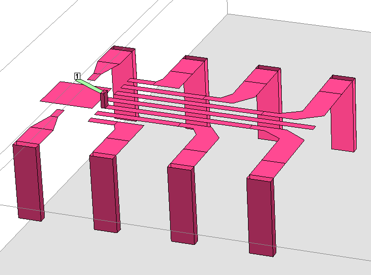
The lead frame internal to a DIP package looks something like the following:

image

Using my new favorite free E&M simulation tool Sonnet (https://www.sonnetsoftware.com/), I drew a crude approximation of the metal interconnect in a DIP14 package.

image

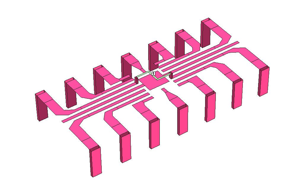
Although it doesn't appear in the 3D preview, I set the lead frame metal to have a thickness of 10 mils. In the free lite edition of Sonnet you are limited to a 3-layer stackup

image

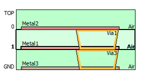
It is what it is, but for small simulation studies, I think it is adequate. The bottom ground layer is a solid ground plane, so all the pins are shorted at the hypothetical PCB landing pads.

For a first pass, I drew the bond wires on the rectangular grid

image

You can draw any geometry you like. However, more complicated geometry requires more complicated and detailed meshing to represent said geometry. Which requires more simulation memory. In the lite edition of Sonnet you are limited to 64 MB.

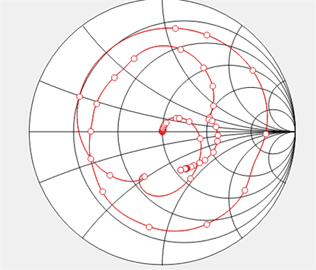
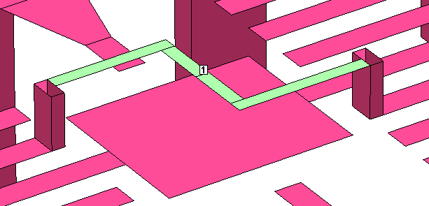
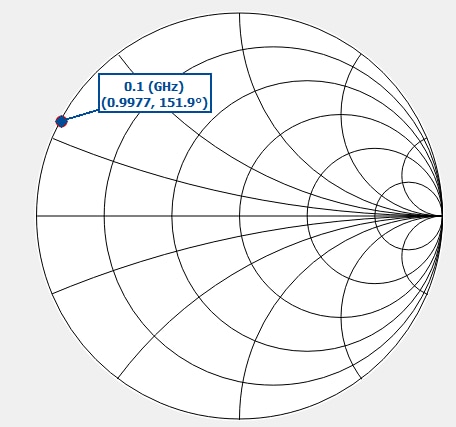
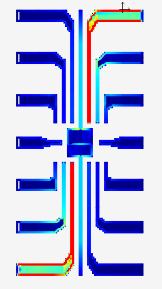
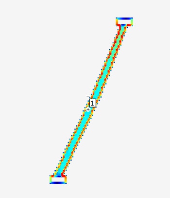
The test feed port is illustrated as the box labeled "1" in the figure above. I ran an S-parameter simulation at 100 MHz. From the perspective of the logic IC we see a short plus some inductance

image

Sonnet has a number of other convenience graphing formats 

image

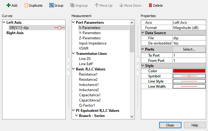
Such as the equivalent inductance 

image

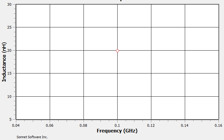
We see a total inductance of 20 nH through both pins 7 and 14, or approximately 10 nH per corner lead. Here is the current distribution in the lead frame at 100 MHz

image

We could also simplify the geometry removing all addition pins and generate a much finer mesh.

image

In this case, I ended up with a memory requirement of 47 MB, just below the 64 MB limit, with:

image

image image 

image 

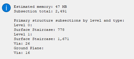
With the alternate bond wire geometry and additional mesh resolution an inductance of 18.5 nH was simulated. 

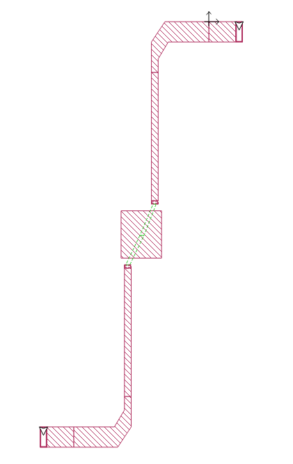
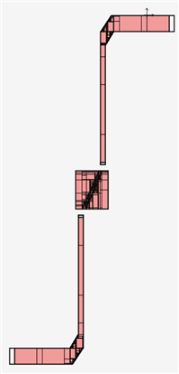
Another approach is simulate just half the package, using a wall referenced feed port

image

Similar to the other 2 simulations, this third simulation resulted in a corner lead inductance of 9.3 nH.

I know there are lots of E&M simulation tools out there, this is just a "free" one I am experimenting with.

Pretty neat.

  • Sign in to reply
  • Cancel

Top Replies

  • colporteur
    colporteur over 1 year ago +3
    Way cool presentation. College quality lecture material.
  • scottiebabe
    scottiebabe over 1 year ago +2
    Hopefully in the future I can show a time domain representation of the extracted s-parameters. Of say, a trace crossing a ground slot
  • genebren
    genebren over 1 year ago +1
    Very cool! Interesting tool, producing some nice graphics.
  • genebren
    genebren over 1 year ago

    Very cool!  Interesting tool, producing some nice graphics.

    • Cancel
    • Vote Up +1 Vote Down
    • Sign in to reply
    • Cancel
  • javagoza
    javagoza over 1 year ago

    Very interesting, as always. Sonnet software should give you a professional license for all the road tests you are doing.

    • Cancel
    • Vote Up +1 Vote Down
    • Sign in to reply
    • Cancel
  • colporteur
    colporteur over 1 year ago

    Way cool presentation. College quality lecture material.

    • Cancel
    • Vote Up +3 Vote Down
    • Sign in to reply
    • Cancel
  • scottiebabe
    scottiebabe over 1 year ago in reply to javagoza

    Thanks as always for the kind words. I am just grateful Sonnet has a free edition for individuals to experiment with. It is quite neat to see signals at such high frequencies.

    • Cancel
    • Vote Up +1 Vote Down
    • Sign in to reply
    • Cancel
  • scottiebabe
    scottiebabe over 1 year ago in reply to colporteur

    Thank you for the high marks, but I have to give credit to the EDA tool. Its almost as easy as MS Paint + LTSpice...

    • Cancel
    • Vote Up +1 Vote Down
    • Sign in to reply
    • Cancel
  • scottiebabe
    scottiebabe over 1 year ago

    Hopefully in the future I can show a time domain representation of the extracted s-parameters. Of say, a trace crossing a ground slot

    image

    image

    • Cancel
    • Vote Up +2 Vote Down
    • Sign in to reply
    • Cancel
  • DAB
    DAB over 1 year ago

    Your blog explains why we saw interesting effects when we got to high frequency digital designs.

    • Cancel
    • Vote Up +1 Vote Down
    • Sign in to reply
    • Cancel
element14 Community

element14 is the first online community specifically for engineers. Connect with your peers and get expert answers to your questions.

  • Members
  • Learn
  • Technologies
  • Challenges & Projects
  • Products
  • Store
  • About Us
  • Feedback & Support
  • FAQs
  • Terms of Use
  • Privacy Policy
  • Legal and Copyright Notices
  • Sitemap
  • Cookies

An Avnet Company © 2025 Premier Farnell Limited. All Rights Reserved.

Premier Farnell Ltd, registered in England and Wales (no 00876412), registered office: Farnell House, Forge Lane, Leeds LS12 2NE.

ICP 备案号 10220084.

Follow element14

  • X
  • Facebook
  • linkedin
  • YouTube