element14 Community
element14 Community
    Register Log In
  • Site
  • Search
  • Log In Register
  • About Us
  • Community Hub
    Community Hub
    • What's New on element14
    • Feedback and Support
    • Benefits of Membership
    • Personal Blogs
    • Members Area
    • Achievement Levels
  • Learn
    Learn
    • Ask an Expert
    • eBooks
    • element14 presents
    • Learning Center
    • Tech Spotlight
    • STEM Academy
    • Webinars, Training and Events
    • Learning Groups
  • Technologies
    Technologies
    • 3D Printing
    • FPGA
    • Industrial Automation
    • Internet of Things
    • Power & Energy
    • Sensors
    • Technology Groups
  • Challenges & Projects
    Challenges & Projects
    • Design Challenges
    • element14 presents Projects
    • Project14
    • Arduino Projects
    • Raspberry Pi Projects
    • Project Groups
  • Products
    Products
    • Arduino
    • Avnet Boards Community
    • Dev Tools
    • Manufacturers
    • Multicomp Pro
    • Product Groups
    • Raspberry Pi
    • RoadTests & Reviews
  • Store
    Store
    • Visit Your Store
    • Choose another store...
      • Europe
      •  Austria (German)
      •  Belgium (Dutch, French)
      •  Bulgaria (Bulgarian)
      •  Czech Republic (Czech)
      •  Denmark (Danish)
      •  Estonia (Estonian)
      •  Finland (Finnish)
      •  France (French)
      •  Germany (German)
      •  Hungary (Hungarian)
      •  Ireland
      •  Israel
      •  Italy (Italian)
      •  Latvia (Latvian)
      •  
      •  Lithuania (Lithuanian)
      •  Netherlands (Dutch)
      •  Norway (Norwegian)
      •  Poland (Polish)
      •  Portugal (Portuguese)
      •  Romania (Romanian)
      •  Russia (Russian)
      •  Slovakia (Slovak)
      •  Slovenia (Slovenian)
      •  Spain (Spanish)
      •  Sweden (Swedish)
      •  Switzerland(German, French)
      •  Turkey (Turkish)
      •  United Kingdom
      • Asia Pacific
      •  Australia
      •  China
      •  Hong Kong
      •  India
      •  Korea (Korean)
      •  Malaysia
      •  New Zealand
      •  Philippines
      •  Singapore
      •  Taiwan
      •  Thailand (Thai)
      • Americas
      •  Brazil (Portuguese)
      •  Canada
      •  Mexico (Spanish)
      •  United States
      Can't find the country/region you're looking for? Visit our export site or find a local distributor.
  • Translate
  • Profile
  • Settings
PCB Design, Prototyping and Production
  • Products
  • More
PCB Design, Prototyping and Production
PCB Forum Let's talk about Crosstalk !
  • Blog
  • Forum
  • Documents
  • Leaderboard
  • Files
  • Members
  • Mentions
  • Sub-Groups
  • Tags
  • More
  • Cancel
  • New
Join PCB Design, Prototyping and Production to participate - click to join for free!
Actions
  • Share
  • More
  • Cancel
Forum Thread Details
  • Replies 36 replies
  • Subscribers 122 subscribers
  • Views 3265 views
  • Users 0 members are here
  • cross-talk
  • frequency_generator
  • pcb
  • oscilloscope
  • spectrum_analyzer
  • debugging
Related

Let's talk about Crosstalk !

battlecoder
battlecoder over 1 year ago

I've been a member for a long time, but this is my first time posting.

I guess it's a bit too late for a presentation, but I'm a software engineer with a fascination for electronics; It's been my hobby for more than 20 years, and I keep learning new things almost every day.

I recently became interested in frequency domain analysis. I know it has countless applications in the Ham/radio world, but I was thinking about more general-purpose use cases; like identifying cross-talk or interference on a PCB design.

I know that's a huge topic and there's some well known general advice and practices to reduce this, like ground planes and decoupling capacitors, and filters... but I wanted to check how bad it could be, if absolutely no sane advice or practice was followed.

So I came up with this ugly PCB as my ultimate test-bed:

image

This is honestly not far from a PCB I would have designed when I was starting in electronics. I liked having nothing but the tracks on the board.

For a first test, I injected two signals from a signal generator on the left side of the PCB, both very stable and clean. One of them a 7 Mhz sine wave, and the other one a 10 Mhz square wave. I picked two relatively close frequencies to see how easy (or hard) was going to be telling them apart later.

Both traces start very far from each other on the left side of the PCB on big pads, and then they get closer together near the center, just to take on their own separate paths again as their approach the right side.

I'm monitoring the "output pad" on the right side for both waveforms on an oscilloscope, and while I was initially watching both on the screen of the scope, the one that I think looked more interesting was the output of the "sine wave" trace:

image

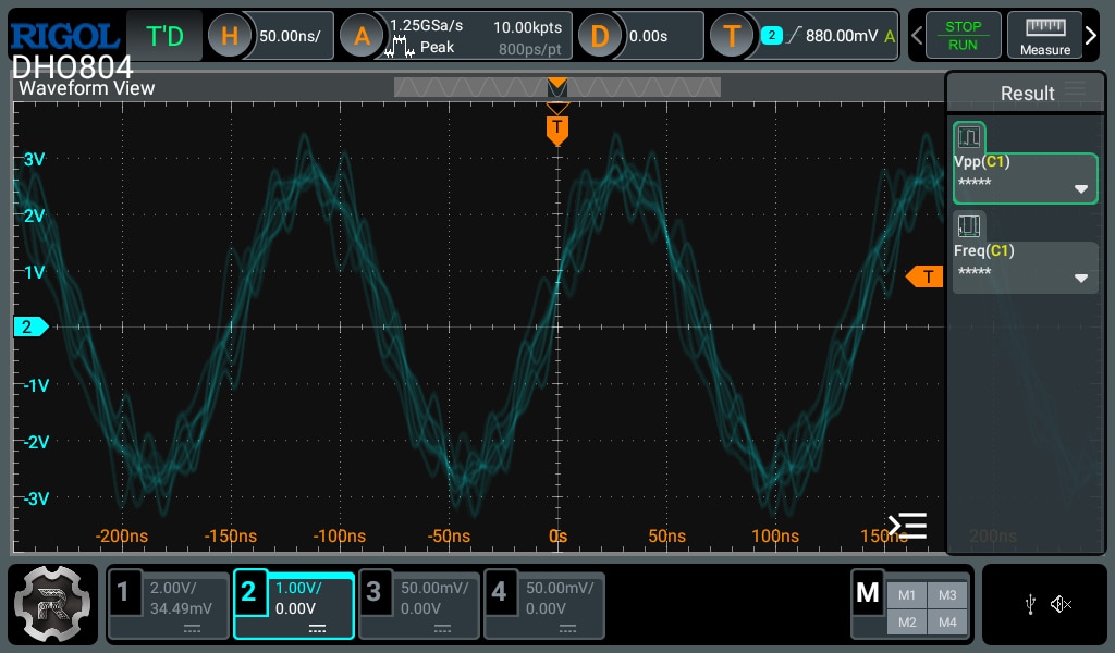
That's one messed up sine wave. For the record; without the square wave signal connected (or with the signal turned off), that wobbly sine-wave becomes a very clean, proper sinusoidal wave, so this was clearly the influence of the other signal.

I'm sure it's possible to use the FFT on the scope to dissect the frequency content of that signal,but I wanted to explore none-invasive methods. Something that I could use for a quick inspection and that didn't require probing around test points or component pins. Something that could potentially identify higher-frequency content outside of the range of my scope. And for that  I went for a cheap "near field" probe, connected to a TinySA Ultra Spectrum Analyzer. You can actually see the near field "probe" hovering over the tracks in the first picture.

This is a capture from the TinySA:

image

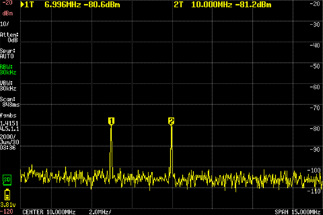
I was honestly amazed at how well this worked. The probe captured perfectly the two main components of the coupled signal (both a 7 and a 10 Mhz component) even without touching the PCB. Because I zoomed tightly on the frequency range of both signals there's no harmonics from the square wave in sight.

The results were pretty exciting to me, but this left me curious about a couple of things. And I thought this forum was the perfect place to ask::

How often is this kind of debugging needed in real life? How frequently is this kind of analysis required? (other than when performing EMI emissions testing). Is there an area in electronics where cross-talk issues are more of a problem than in others? (for example is this problem worse in high-frequency applications?)

If any of you have an anecdote or story where cross-talk has been an issue, a mystery, or a lesson well learned, I'd love to hear it!

  • Sign in to reply
  • Cancel

Top Replies

  • genebren
    genebren over 1 year ago in reply to battlecoder +4
    I found the book that I was referring to, "Mixed-Signal Hardware and Housekeeping Techniques" by Walt Kester of Analog Devices. This was a part of the handout for a seminar session that I attended on dealing…
  • cstanton
    cstanton over 1 year ago +3
    battlecoder said: How frequently is this kind of analysis required? When you start discussing crosstalk, you perhaps also start delving into the concepts and implications of information leakage, what…
  • battlecoder
    battlecoder over 1 year ago in reply to e14phil +3
    Thanks! I've been meaning to write here for a while, but I couldn't find something interesting to write about. When I decided to experiment with this I figured it would be great to have input from actual…
Parents
  • Andrew J
    Andrew J over 1 year ago

    I don’t have an answer but it’s an interesting experiment to post about.  Are you sharing the ground paths between the two signals?  What happens if you don’t?  What happens as the frequencies get further apart / closer together?

    • Cancel
    • Vote Up +1 Vote Down
    • Sign in to reply
    • Cancel
  • shabaz
    shabaz over 1 year ago in reply to Andrew J

    I think it's that lower trace in the photo, which is the ground path. Actually, one more experiment the OP could do, is swap the probe and croc-clip connections to make that ground path become the central trace instead of the lower one. Might improve things a bit, but really needs a ground plane.

    • Cancel
    • Vote Up +1 Vote Down
    • Sign in to reply
    • Cancel
  • Andrew J
    Andrew J over 1 year ago in reply to shabaz

    I think the OP is just experimenting to MAKE crosstalk and see how bad it is, rather than asking why.  There's also the top unused trace.  

    I thought it could be interesting to create a PCB that had a variety of paths, e.g.

    • As per the OP: two signal paths that converge/diverge with a common ground
    • two signal paths that converge but have a  separate return between them
    • two signal paths that converge but have a separate return on the bottom side that lie directly under the signal path
    • two signal paths that converge but have a single (common) ground plane underneath them.
    • two signal paths directly over each other with a separate ground plane on the inner two layers (requires a 4 layer PCB)

    I suppose there are a number of combinations but it would be easy to experiment to see how signals are affected with these layouts at different frequency distances.

    As for the OPs original questions, I don't know as I don't have any experience to draw on.

    • Cancel
    • Vote Up +1 Vote Down
    • Sign in to reply
    • Cancel
Reply
  • Andrew J
    Andrew J over 1 year ago in reply to shabaz

    I think the OP is just experimenting to MAKE crosstalk and see how bad it is, rather than asking why.  There's also the top unused trace.  

    I thought it could be interesting to create a PCB that had a variety of paths, e.g.

    • As per the OP: two signal paths that converge/diverge with a common ground
    • two signal paths that converge but have a  separate return between them
    • two signal paths that converge but have a separate return on the bottom side that lie directly under the signal path
    • two signal paths that converge but have a single (common) ground plane underneath them.
    • two signal paths directly over each other with a separate ground plane on the inner two layers (requires a 4 layer PCB)

    I suppose there are a number of combinations but it would be easy to experiment to see how signals are affected with these layouts at different frequency distances.

    As for the OPs original questions, I don't know as I don't have any experience to draw on.

    • Cancel
    • Vote Up +1 Vote Down
    • Sign in to reply
    • Cancel
Children
  • battlecoder
    battlecoder over 1 year ago in reply to Andrew J

    You are correct! bottom trace is ground in the test setup. I also added a top trace in case I wanted to experiment with adding a second ground path at top. Using one of the middle traces as ground is another completely valid experiment, but as Andrew mentioned, I first tried to make crosstalk happen, which is also the reason why I didn't add a ground plane to begin with.

    I like the idea of creating a PCB with variety of paths. Like a sort of cross-talk educational board!

    • Cancel
    • Vote Up 0 Vote Down
    • Sign in to reply
    • Cancel
element14 Community

element14 is the first online community specifically for engineers. Connect with your peers and get expert answers to your questions.

  • Members
  • Learn
  • Technologies
  • Challenges & Projects
  • Products
  • Store
  • About Us
  • Feedback & Support
  • FAQs
  • Terms of Use
  • Privacy Policy
  • Legal and Copyright Notices
  • Sitemap
  • Cookies

An Avnet Company © 2025 Premier Farnell Limited. All Rights Reserved.

Premier Farnell Ltd, registered in England and Wales (no 00876412), registered office: Farnell House, Forge Lane, Leeds LS12 2NE.

ICP 备案号 10220084.

Follow element14

  • X
  • Facebook
  • linkedin
  • YouTube