element14 Community
element14 Community
    Register Log In
  • Site
  • Search
  • Log In Register
  • About Us
  • Community Hub
    Community Hub
    • What's New on element14
    • Feedback and Support
    • Benefits of Membership
    • Personal Blogs
    • Members Area
    • Achievement Levels
  • Learn
    Learn
    • Ask an Expert
    • eBooks
    • element14 presents
    • Learning Center
    • Tech Spotlight
    • STEM Academy
    • Webinars, Training and Events
    • Learning Groups
  • Technologies
    Technologies
    • 3D Printing
    • FPGA
    • Industrial Automation
    • Internet of Things
    • Power & Energy
    • Sensors
    • Technology Groups
  • Challenges & Projects
    Challenges & Projects
    • Design Challenges
    • element14 presents Projects
    • Project14
    • Arduino Projects
    • Raspberry Pi Projects
    • Project Groups
  • Products
    Products
    • Arduino
    • Avnet Boards Community
    • Dev Tools
    • Manufacturers
    • Multicomp Pro
    • Product Groups
    • Raspberry Pi
    • RoadTests & Reviews
  • Store
    Store
    • Visit Your Store
    • Choose another store...
      • Europe
      •  Austria (German)
      •  Belgium (Dutch, French)
      •  Bulgaria (Bulgarian)
      •  Czech Republic (Czech)
      •  Denmark (Danish)
      •  Estonia (Estonian)
      •  Finland (Finnish)
      •  France (French)
      •  Germany (German)
      •  Hungary (Hungarian)
      •  Ireland
      •  Israel
      •  Italy (Italian)
      •  Latvia (Latvian)
      •  
      •  Lithuania (Lithuanian)
      •  Netherlands (Dutch)
      •  Norway (Norwegian)
      •  Poland (Polish)
      •  Portugal (Portuguese)
      •  Romania (Romanian)
      •  Russia (Russian)
      •  Slovakia (Slovak)
      •  Slovenia (Slovenian)
      •  Spain (Spanish)
      •  Sweden (Swedish)
      •  Switzerland(German, French)
      •  Turkey (Turkish)
      •  United Kingdom
      • Asia Pacific
      •  Australia
      •  China
      •  Hong Kong
      •  India
      •  Korea (Korean)
      •  Malaysia
      •  New Zealand
      •  Philippines
      •  Singapore
      •  Taiwan
      •  Thailand (Thai)
      • Americas
      •  Brazil (Portuguese)
      •  Canada
      •  Mexico (Spanish)
      •  United States
      Can't find the country/region you're looking for? Visit our export site or find a local distributor.
  • Translate
  • Profile
  • Settings
PCB Design, Prototyping and Production
  • Products
  • More
PCB Design, Prototyping and Production
PCB Forum PCB design - Question from schematic to PCB | Kicad
  • Blog
  • Forum
  • Documents
  • Leaderboard
  • Files
  • Members
  • Mentions
  • Sub-Groups
  • Tags
  • More
  • Cancel
  • New
Join PCB Design, Prototyping and Production to participate - click to join for free!
Actions
  • Share
  • More
  • Cancel
Forum Thread Details
  • State Not Answered
  • Replies 14 replies
  • Subscribers 118 subscribers
  • Views 1881 views
  • Users 0 members are here
  • kicad
Related

PCB design - Question from schematic to PCB | Kicad

feiticeir0
feiticeir0 over 1 year ago

Hi all !

I'm coming to you with, probably, a newby question from PCB design.

I'm trying to design my second PCB (the first one had a flaw that I didn't foresaw and was a bust) and I'm coming to you for a small verification.

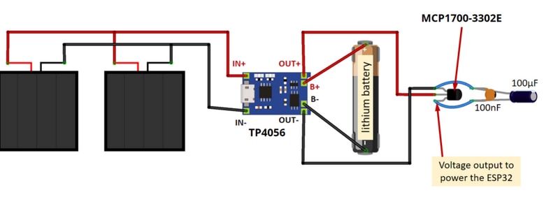
I'm trying to design a PCB for the following circuit (from https://randomnerdtutorials.com/power-esp32-esp8266-solar-panels-battery-level-monitoring/:

image

I'm going to use a ESP32-CAM .

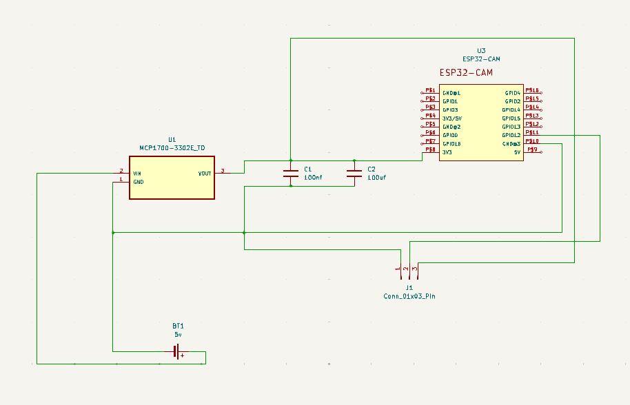
I already have the kicad project done - the schematics:
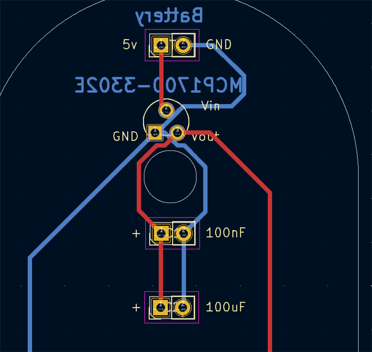
image

and the PCB layout:

image

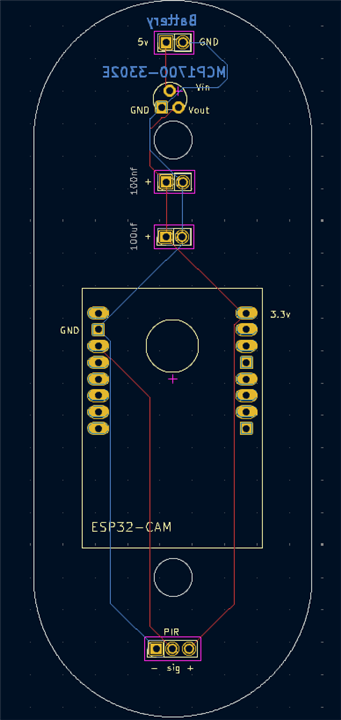
Now, my question is regarding the wiring from the battery to the two capacitors and then to the ESP32-CAM. Will the wiring, like it is, be the same like in Fritzing design ?

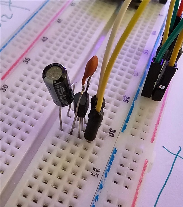
I have this working on a breadboard - but there I wire all the wires on the same rail -

image

Thank you

  • Sign in to reply
  • Cancel

Top Replies

  • Jan Cumps
    Jan Cumps over 1 year ago in reply to Jan Cumps +3
    Zones are a bit odd, until you managed to use them once. Maybe create a project with just Vss, Vdd and two resistors in parallel. Then try to play with zones on the PCB design of that simple example. …
  • Jan Cumps
    Jan Cumps over 1 year ago in reply to feiticeir0 +2
    When you add the zone, give it the same net name as the pads that you try to connect.
  • feiticeir0
    feiticeir0 over 1 year ago in reply to shabaz +1
    Thank you ! I'm not even considering the TP4056 for the PCB - that will be connected to the solar panels. This PCB will only be from output of the TP4056 - it will be connected to the battery holes.…
Parents
  • feiticeir0
    0 feiticeir0 over 1 year ago

    Thank you for the replies.

    I will increase the trace width and moved it a bit from the unconnected pads.

    I've changed the layout a bit, so now I have this:

    image

    This way it mimics better all the capacitors being connected to the MCP17000. I'm guessing it's ok.

    Is there any way to test this ? Some kind of simulator ?

    Thank you

    • Cancel
    • Vote Up 0 Vote Down
    • Sign in to reply
    • Verify Answer
    • Cancel
  • dougw
    0 dougw over 1 year ago in reply to feiticeir0

    The automated design rule check should tell you if there are problems. The ground traces still look like they are touching the input and output pads  of the regulator.

    • Cancel
    • Vote Up 0 Vote Down
    • Sign in to reply
    • Verify Answer
    • Cancel
  • feiticeir0
    0 feiticeir0 over 1 year ago in reply to dougw

    I have two cooper layers.  The ground is on one layer and the voltage is on another layer.

    Thank you for the replies !

    • Cancel
    • Vote Up 0 Vote Down
    • Sign in to reply
    • Verify Answer
    • Cancel
Reply
  • feiticeir0
    0 feiticeir0 over 1 year ago in reply to dougw

    I have two cooper layers.  The ground is on one layer and the voltage is on another layer.

    Thank you for the replies !

    • Cancel
    • Vote Up 0 Vote Down
    • Sign in to reply
    • Verify Answer
    • Cancel
Children
No Data
element14 Community

element14 is the first online community specifically for engineers. Connect with your peers and get expert answers to your questions.

  • Members
  • Learn
  • Technologies
  • Challenges & Projects
  • Products
  • Store
  • About Us
  • Feedback & Support
  • FAQs
  • Terms of Use
  • Privacy Policy
  • Legal and Copyright Notices
  • Sitemap
  • Cookies

An Avnet Company © 2025 Premier Farnell Limited. All Rights Reserved.

Premier Farnell Ltd, registered in England and Wales (no 00876412), registered office: Farnell House, Forge Lane, Leeds LS12 2NE.

ICP 备案号 10220084.

Follow element14

  • X
  • Facebook
  • linkedin
  • YouTube