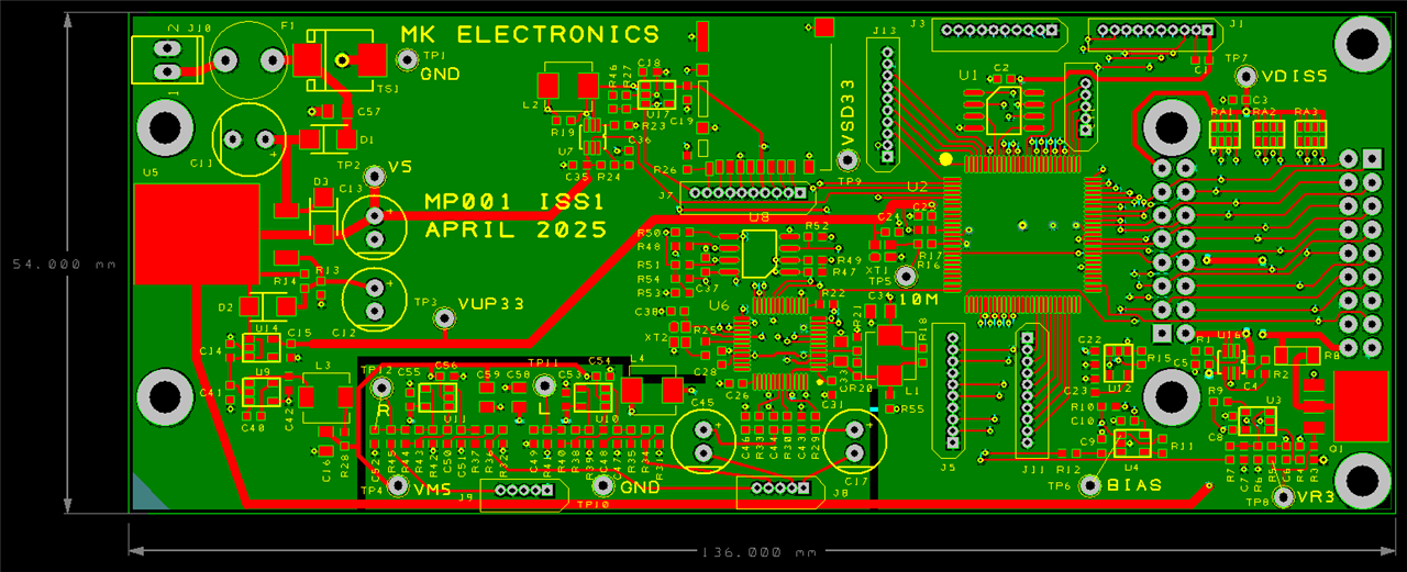
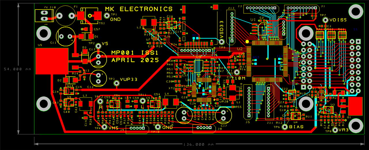
As someone passionate about electronics and embedded systems, I’m always looking for new ways to push the boundaries of PCB design. Whether it's creating compact, high-performance circuits or optimizing power distribution for efficient operation, each project brings unique challenges and learning opportunities.
Right now, I’m excited to work on a new PCB project integrating multiple sensors and wireless communication modules while keeping the design compact and power-efficient. The goal is to build a reliable and scalable solution that can be used for IoT applications, automation, and real-time data processing.
One of the most intriguing aspects of this project is refining the layout to reduce noise and interference while maintaining signal integrity. The use of dedicated ground planes, proper trace routing, and decoupling capacitors plays a critical role in ensuring stable performance. I’m also experimenting with different design software to see which offers the best balance between usability and advanced features.
Another key area I’m focusing on is thermal management. With increasing circuit complexity, managing heat dissipation effectively is crucial. Exploring techniques such as thermal vias, copper pours, and strategic component placement has been an exciting learning experience.
If you’re also into PCB design, I’d love to hear your thoughts! What are some of the biggest challenges you've faced, and what innovative solutions have worked for you? Let’s share ideas and push the limits of what we can create!