element14 Community
element14 Community
    Register Log In
  • Site
  • Search
  • Log In Register
  • Community Hub
    Community Hub
    • What's New on element14
    • Feedback and Support
    • Benefits of Membership
    • Personal Blogs
    • Members Area
    • Achievement Levels
  • Learn
    Learn
    • Ask an Expert
    • eBooks
    • element14 presents
    • Learning Center
    • Tech Spotlight
    • STEM Academy
    • Webinars, Training and Events
    • Learning Groups
  • Technologies
    Technologies
    • 3D Printing
    • FPGA
    • Industrial Automation
    • Internet of Things
    • Power & Energy
    • Sensors
    • Technology Groups
  • Challenges & Projects
    Challenges & Projects
    • Design Challenges
    • element14 presents Projects
    • Project14
    • Arduino Projects
    • Raspberry Pi Projects
    • Project Groups
  • Products
    Products
    • Arduino
    • Avnet & Tria Boards Community
    • Dev Tools
    • Manufacturers
    • Multicomp Pro
    • Product Groups
    • Raspberry Pi
    • RoadTests & Reviews
  • About Us
    About the element14 Community
  • Store
    Store
    • Visit Your Store
    • Choose another store...
      • Europe
      •  Austria (German)
      •  Belgium (Dutch, French)
      •  Bulgaria (Bulgarian)
      •  Czech Republic (Czech)
      •  Denmark (Danish)
      •  Estonia (Estonian)
      •  Finland (Finnish)
      •  France (French)
      •  Germany (German)
      •  Hungary (Hungarian)
      •  Ireland
      •  Israel
      •  Italy (Italian)
      •  Latvia (Latvian)
      •  
      •  Lithuania (Lithuanian)
      •  Netherlands (Dutch)
      •  Norway (Norwegian)
      •  Poland (Polish)
      •  Portugal (Portuguese)
      •  Romania (Romanian)
      •  Russia (Russian)
      •  Slovakia (Slovak)
      •  Slovenia (Slovenian)
      •  Spain (Spanish)
      •  Sweden (Swedish)
      •  Switzerland(German, French)
      •  Turkey (Turkish)
      •  United Kingdom
      • Asia Pacific
      •  Australia
      •  China
      •  Hong Kong
      •  India
      •  Japan
      •  Korea (Korean)
      •  Malaysia
      •  New Zealand
      •  Philippines
      •  Singapore
      •  Taiwan
      •  Thailand (Thai)
      •  Vietnam
      • Americas
      •  Brazil (Portuguese)
      •  Canada
      •  Mexico (Spanish)
      •  United States
      Can't find the country/region you're looking for? Visit our export site or find a local distributor.
  • Translate
  • Profile
  • Settings
PCB Design, Prototyping and Production
  • Products
  • More
PCB Design, Prototyping and Production
PCB Forum Thermal profile methodology for DIY reflow — what I know, what I'm missing
  • Blog
  • Forum
  • Documents
  • Leaderboard
  • Files
  • Members
  • Mentions
  • Sub-Groups
  • Tags
  • More
  • Cancel
  • New
Join PCB Design, Prototyping and Production to participate - click to join for free!
Actions
  • Share
  • More
  • Cancel
Forum Thread Details
  • Replies 8 replies
  • Subscribers 153 subscribers
  • Views 323 views
  • Users 0 members are here
  • reflow
  • soldering
Related

Thermal profile methodology for DIY reflow — what I know, what I'm missing

pvit
pvit 28 days ago

Hi everyone. I built a compact reflow micro-table for hassle-free PCB assembly at home:  Reflow Micro Table: Compact USB PD Reflow Table with Browser Control 

I'd like to write a general guide on setting up thermal profiles, but I lack the practical experience to make something solid. I'm not talking about production-line requirements — more about "reasonably good" for advanced DIY.

What I know so far as hard constraints:

  • For RoHS/leaded: TAL no more than 60 seconds. For LTS — I'm not sure.
  • Ramp rate: 1–2°C/sec (except the start)
  • Cooling rate: ~4°C/sec; passive air cooling is acceptable (not sure about LTS).

Everything else seems to depend on the specific paste and equipment — recommendations vary widely. The bigger frustration is that datasheets give you a profile to follow but don't explain how much the parameters can actually vary. It's like the difference between a datasheet and a reference manual :)

A colleague with hands-on production experience described this simplified approach to me — I'd be curious whether it holds up in practice:

  • Ramp linearly at 1–2°C/sec
  • Wait until paste visibly melts across all components
  • Turn off immediately and let it cool

I'm keeping the scope to LTS and leaded — RoHS/SAC peak temperatures and tighter process windows are an unnecessary complication for beginners.

Questions

  • How important is a soaking plateau, and how does it depend on the paste type?
  • How long can components and the board stay above a given temperature before damage becomes a concern?
  • Is there a minimum time above liquidus required for proper intermetallic formation?
  • How critical is cooling rate — does the solidification speed affect joint quality, and what is generally preferable?
  • and so on...

I'd really appreciate input from people with real PCB assembly experience to help systematize the practical nuances — the goal is to put together beginner-friendly guidance on building reflow profiles from scratch.


I've also tried to document my limited experience with LTS pastes here: github.com/.../soldering_paste.md — feedback on what could be improved there would be much appreciated as well.

  • Sign in to reply
  • Cancel

Top Replies

  • wolfgangfriedrich
    wolfgangfriedrich 28 days ago +4
    The colleague's method work well for me with an extra step to carefully push the soldered board off the plate after turning off. My plate has enough heat capacitance that the cool down rate is way too…
  • michaelkellett
    michaelkellett 28 days ago +3
    For low volume home or prototype assembly I have found no value at all in setting profiles. All the following is based on leaded solder - I have avoided lead free except for a few occasions using the…
  • pvit
    pvit 28 days ago in reply to wolfgangfriedrich +1
    Personally, I have nothing against lead-free processes. But there are technical limits - existing power does not allow to reach desired ramp up speed for lead free. It's possible to reduce working area…
  • wolfgangfriedrich
    wolfgangfriedrich 28 days ago

    The colleague's method work well for me with an extra step to carefully push the soldered board off the plate after turning off. My plate has enough heat capacitance that the cool down rate is way too slow.

    On your plate (very nice and clean design btw), I would be interested in the temperature difference between your calculated temperature and the temperature on the top side of the board to be soldered. My experience is that the top temp always lags a few degrees behind the plate temp itself. If you want/need to be profile correct, this difference matters and needs to be taken into account. 

    To your questions:

    The soaking plateau gets more important the more copper you have in your board. A 2-layer board is very forgiving, but 4 or 6 layers are happier with the soak to get a more even temperature when ramping up into the liquid phase. Also prevents tombstoning. 

    Max temperature is mainly a concern of the FR4 material used, components are quite robust and have a little convection cooling working for them. The standard FR4 with Tg = 130degC of the cheapest offerings of your favourite Three-Letter board house works OK for one cycle of leaded solder profile. A lead-free profile with temperature up to 260 degC requires Tg of 170degC or better. The substrate gets brittle with compromised structural integrity.

    Cooling rate is again a concern of tombstoning as a slower rate gets more uneven cooling. 5 or 6 degC/sec is preferred over slower rate. 

    And don't be afraid of lead-free solder process, it is no different when you use quality ingredients (as long as we are not talking low temperature solder). 

    • Cancel
    • Vote Up +4 Vote Down
    • Sign in to reply
    • Cancel
  • pvit
    pvit 28 days ago in reply to wolfgangfriedrich

    Personally, I have nothing against lead-free processes. But there are technical limits - existing power does not allow to reach desired ramp up speed for lead free. It's possible to reduce working area, but then comparison with MHP50 will be less impressive :). And as you noted, after additional temperature correction, to compensate losses, things may become too risky.

    wolfgangfriedrich said:
    I would be interested in the temperature difference between your calculated temperature and the temperature on the top side of the board to be soldered

    According to cheap chinese thermal imager, and visual inspection of paste melting, in static state and 4-layer board with power polygons inside

    • about 10-15°C with LTS profile
    • about 20°C with leaded profile
    And with notable delays on ramp up. As you can see on video, bottom right corner - one pin of buzzer is melted even after cooling phase started (probably it was located on corner screw hole). But this is very heavy scenario for "home use". Self-assembly is more acrobatics than normal use :)
    Profiles are already adjusted - the leaded one has 230°C top instead 205°C. Probably, this can be more optimized, but this require more experience than I have in this area.
    • Cancel
    • Vote Up +1 Vote Down
    • Sign in to reply
    • Cancel
  • michaelkellett
    michaelkellett 28 days ago

    For low volume home or prototype assembly I have found no value at all in setting profiles.

    All the following is based on leaded solder - I have avoided lead free except for a few occasions using the CIF IR machine.

    I currently mainly use a fairly expensive (CIF FT03 IR oven with internal air blowers) but before that I used under board hot air or a hot plate.

    With the under board hot air (and a very cheap air blower) you have almost no control over the pcb temperature so the technique is to observe the solder paste and wait until it flows at all points on the board, then give a bit longer for luck. This process is not very repeatable Slight smile and I have known it to kill chips.

    My hotplate technique used a cheap commercial hot plate. Set it to 30 - 50C above the solder melting point. Let it reach stability and place the board on it. Wait for the solder paste to flow - and then give it a bit longer. 

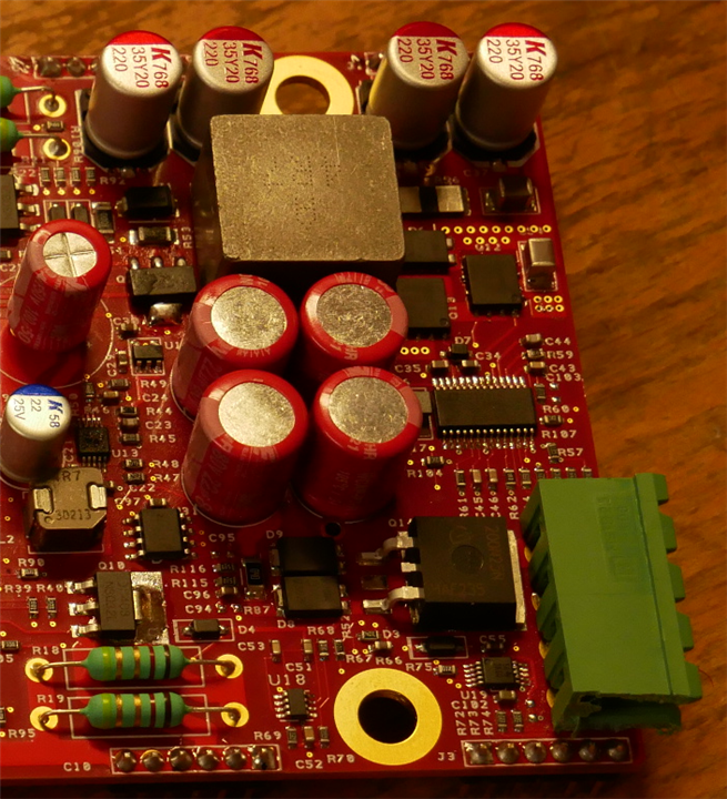
    Recently the CIF failed to flow a board with my usual profile because of the presence of a very large surface mount inductor.

    image

    The big SM Inductor and parts to the right of it and two of the SM capacitors did not solder in the IR oven using my standard reflow profile.

    Rather than scrap the boards I used the hotplate on the corner of the board  - considerable patience was required to reflow the inductor but the knowledge that the boards were scrap without soldering the inductor made me brave. The process worked and none of the other parts seem to have suffered.

    Using a hotplate like this is very much affected by the heat transfer between plate and board. It is necessary to press the board down on the hotplate since it will almost certainly warp as it heats up.

    The advantage of this process is that it can be used when you will only make (or salvage) one board and do not wish to scrap any. Developing a good profile requires experimentation. (My CIF machine could reflow the big inductor - I just wasn't willing to scrap a few boards to get there.)

    Your colleagues advice seems mainly good to me if the hotplate can ramp fast with no overshoot - but my hotplate isn't very good at ramping quickly. I've never seen a hotplate that cools fast enough and I favour getting the temperature down by removing the board.

    (Good solder paste and the use of a decent stencil are important !!)

    Putting though holes of a decent size (1mm or more) in the big pads on the underside of chips allows you to check that the solder has flowed under the chip and may allow you to remove the chip if you have to.

    MK

    • Cancel
    • Vote Up +3 Vote Down
    • Sign in to reply
    • Cancel
  • pvit
    pvit 28 days ago in reply to michaelkellett

    In current configuration the ramp  up is ~ 1°C/sec in high point. Cool down ~ 1°C/sec until go below TAL, then become slower and very slow at room temp.

    • Cancel
    • Vote Up 0 Vote Down
    • Sign in to reply
    • Cancel
  • wolfgangfriedrich
    wolfgangfriedrich 27 days ago in reply to pvit

    When I did have my DIY hot plate, I recorded some temperature profiles. With just turning of and convection cooling, the down ramp was never as steep a decline as the required profile. And the up-ramp was basically linear if there is not enough power or too much mass to heat. 

    (+) Arduino Hot Plate (2) - What's for dessert? - element14 Community

    • Cancel
    • Vote Up 0 Vote Down
    • Sign in to reply
    • Cancel
  • wolfgangfriedrich
    wolfgangfriedrich 27 days ago in reply to michaelkellett
    michaelkellett said:
    Using a hotplate like this is very much affected by the heat transfer between plate and board. It is necessary to press the board down on the hotplate since it will almost certainly warp as it heats up.

    This is probably the most important point to make a hot-plate work, at least when frying larger boards. 

    • Cancel
    • Vote Up 0 Vote Down
    • Sign in to reply
    • Cancel
  • pvit
    pvit 27 days ago in reply to wolfgangfriedrich

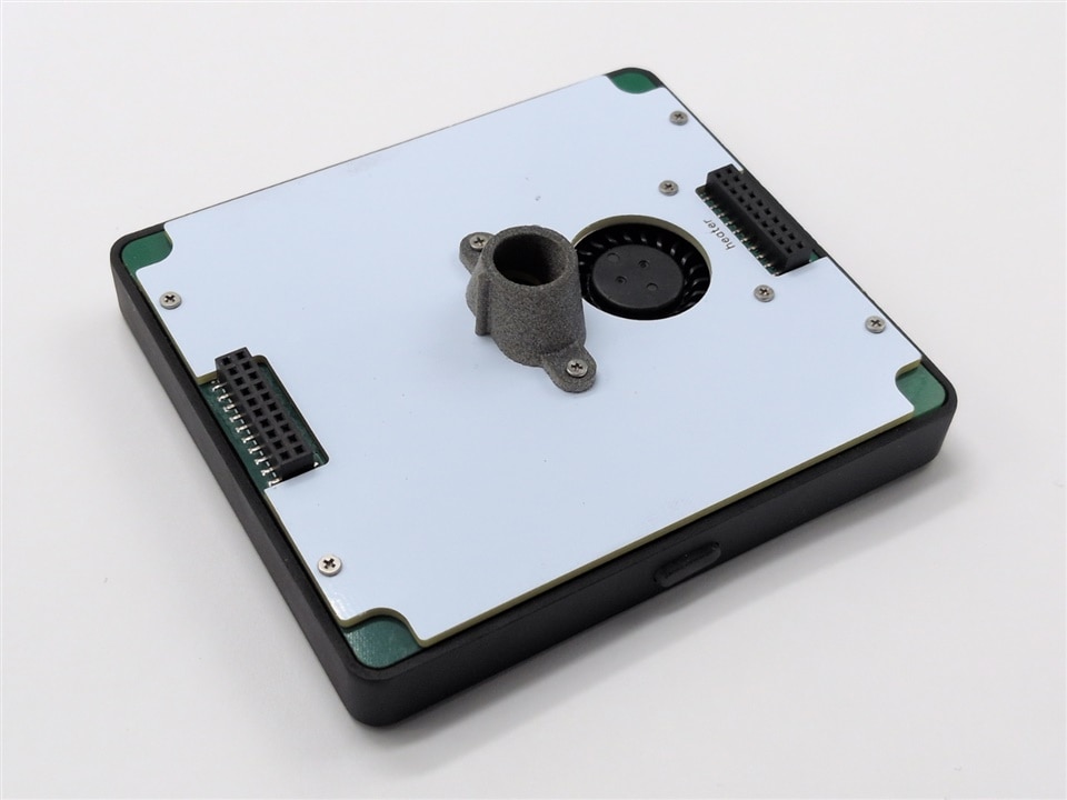
    Yeah. Thin plate => bad heat distribution. Fat plate => slow cooling. I use Pi5 fan to blow from the bottom. It improves cooling speed 2x-3x until melting point reached. But that's still 1°C/sec. Something more serious will not fit device size.

    The cheat is to end profile graph on melting point instead of room temp, lol :).

    image

    • Cancel
    • Vote Up 0 Vote Down
    • Sign in to reply
    • Cancel
  • BigG
    BigG 24 days ago in reply to wolfgangfriedrich

    An idea I had (needs effort to explore practical implications) is to place a layer of densely packed steel wool between the plate and the board to allow for warping and to provide a more even heat distribution. The thermal conductivity of steel wool will certainly be better than air but not as good as a solid metal plate.

    • Cancel
    • Vote Up +1 Vote Down
    • Sign in to reply
    • Cancel
element14 Community

element14 is the first online community specifically for engineers. Connect with your peers and get expert answers to your questions.

  • Members
  • Learn
  • Technologies
  • Challenges & Projects
  • Products
  • Store
  • About Us
  • Feedback & Support
  • FAQs
  • Terms of Use
  • Privacy Policy
  • Legal and Copyright Notices
  • Sitemap
  • Cookies

An Avnet Company © 2026 Premier Farnell Limited. All Rights Reserved.

Premier Farnell Ltd, registered in England and Wales (no 00876412), registered office: Farnell House, Forge Lane, Leeds LS12 2NE.

ICP 备案号 10220084.

Follow element14

  • X
  • Facebook
  • linkedin
  • YouTube