element14 Community
element14 Community
    Register Log In
  • Site
  • Search
  • Log In Register
  • Community Hub
    Community Hub
    • What's New on element14
    • Feedback and Support
    • Benefits of Membership
    • Personal Blogs
    • Members Area
    • Achievement Levels
  • Learn
    Learn
    • Ask an Expert
    • eBooks
    • element14 presents
    • Learning Center
    • Tech Spotlight
    • STEM Academy
    • Webinars, Training and Events
    • Learning Groups
  • Technologies
    Technologies
    • 3D Printing
    • FPGA
    • Industrial Automation
    • Internet of Things
    • Power & Energy
    • Sensors
    • Technology Groups
  • Challenges & Projects
    Challenges & Projects
    • Design Challenges
    • element14 presents Projects
    • Project14
    • Arduino Projects
    • Raspberry Pi Projects
    • Project Groups
  • Products
    Products
    • Arduino
    • Avnet & Tria Boards Community
    • Dev Tools
    • Manufacturers
    • Multicomp Pro
    • Product Groups
    • Raspberry Pi
    • RoadTests & Reviews
  • About Us
    About the element14 Community
  • Store
    Store
    • Visit Your Store
    • Choose another store...
      • Europe
      •  Austria (German)
      •  Belgium (Dutch, French)
      •  Bulgaria (Bulgarian)
      •  Czech Republic (Czech)
      •  Denmark (Danish)
      •  Estonia (Estonian)
      •  Finland (Finnish)
      •  France (French)
      •  Germany (German)
      •  Hungary (Hungarian)
      •  Ireland
      •  Israel
      •  Italy (Italian)
      •  Latvia (Latvian)
      •  
      •  Lithuania (Lithuanian)
      •  Netherlands (Dutch)
      •  Norway (Norwegian)
      •  Poland (Polish)
      •  Portugal (Portuguese)
      •  Romania (Romanian)
      •  Russia (Russian)
      •  Slovakia (Slovak)
      •  Slovenia (Slovenian)
      •  Spain (Spanish)
      •  Sweden (Swedish)
      •  Switzerland(German, French)
      •  Turkey (Turkish)
      •  United Kingdom
      • Asia Pacific
      •  Australia
      •  China
      •  Hong Kong
      •  India
      •  Japan
      •  Korea (Korean)
      •  Malaysia
      •  New Zealand
      •  Philippines
      •  Singapore
      •  Taiwan
      •  Thailand (Thai)
      •  Vietnam
      • Americas
      •  Brazil (Portuguese)
      •  Canada
      •  Mexico (Spanish)
      •  United States
      Can't find the country/region you're looking for? Visit our export site or find a local distributor.
  • Translate
  • Profile
  • Settings
PCB Design, Prototyping and Production
  • Products
  • More
PCB Design, Prototyping and Production
PCB Forum PCBAtlas update: App Store release and Android free trial now available
  • Blog
  • Forum
  • Documents
  • Leaderboard
  • Files
  • Members
  • Mentions
  • Sub-Groups
  • Tags
  • More
  • Cancel
  • New
Join PCB Design, Prototyping and Production to participate - click to join for free!
Actions
  • Share
  • More
  • Cancel
Forum Thread Details
  • Replies 12 replies
  • Subscribers 161 subscribers
  • Views 275 views
  • Users 0 members are here
Related

PCBAtlas update: App Store release and Android free trial now available

EthanKang
EthanKang 1 month ago

Hi everyone,

About a month ago, I introduced PCBAtlas here while the Apple version was still in public TestFlight. I wanted to post a development update now that it has moved into a regular App Store release, and an Android version is also available as a direct free trial.

PCBAtlas is still focused on the same problem: providing a local-first workspace for opening, organizing, and reviewing PCB design and manufacturing data without requiring a full EDA installation or uploading board files to a web service.

It is not intended to replace KiCad, a PCB editor, or a formal CAM/DFM sign-off process. The goal is to make routine inspection, revision review, issue communication, lab work, and manufacturing handoff more convenient.

The current versions support workflows around:

  • KiCad projects, schematics, and .kicad_pcb boards

  • DSN files

  • IPC-2581 XML

  • ODB++ archives and directories

  • Recognized manufacturing-package folders

  • 2D board inspection, object selection, search, and layer controls

  • Project and schematic browsing where available

  • Board-level 3D viewing

  • Managed revisions inside the same PCB workspace

Since the earlier beta, much of the work has been less visible but important: improving large-board rendering, selection on dense layouts, import progress, saved viewer state, repeated open/reopen workflows, ODB++ archive handling, 3D navigation, thumbnails, and general stability.

The Android build now follows the same general review workflow as the Apple versions. It is temporarily available as a direct APK free trial. The download page also publishes the build version, SHA-256 checksum, and signer certificate fingerprint for verification.

image

I am particularly interested in feedback on:

  • Files that fail to import or take unexpectedly long

  • Incorrect or missing layers, shapes, line widths, pads, or vias

  • ODB++ and IPC-2581 compatibility problems

  • Selection problems on dense or overlapping board geometry

  • Whether the revision/workspace model is genuinely useful

  • Information that is still missing during a real review or manufacturing handoff

Website and downloads:

https://www.astroformsoftware.com/

When reporting an issue, the platform, device model, file format, approximate board size, and the import stage where the problem occurred are especially useful. Non-sensitive test files are welcome, but screenshots and descriptions are also helpful.

Disclosure: I am the developer of PCBAtlas. I will keep technical discussion and support public where practical, and I will not send unsolicited DMs or add anyone to a mailing list.

  • Sign in to reply
  • Cancel

Top Replies

  • michaelkellett
    michaelkellett 1 month ago in reply to EthanKang +1
    I don't want to rain on your parade but, Why would any one want to review a PCB on a tablet - I use a 42" 4K screen to do PCB design work I can't imagine attempting it on a tablet. Lots of people use…
  • cstanton
    cstanton 1 month ago in reply to misaz +1
    misaz said: Agree, but how often do such households perform PCB layout reviews? Given most electrical makers I've seen at hackspaces are carrying phones and ipads, I suspect it's higher than you may…
  • shabaz
    shabaz 1 month ago +1
    The video didn't demonstrate much, but the ability to view and explore KiCad projects on desktop or mobile devices is already possible with KiCanvas ( example PCB view ). Example schematic : At…
  • stanto
    stanto 1 month ago

    So the difference to simply using KiCAD is that it's for ios and android?

    • Cancel
    • Vote Up 0 Vote Down
    • Sign in to reply
    • Cancel
  • EthanKang
    EthanKang 1 month ago in reply to stanto

    That is essentially correct for now. PCBAtlas is intended to provide a practical way to review PCB designs on mobile devices, especially tablets, rather than replace KiCad as a full design tool.

    Once the core viewing and review functions are more complete, we plan to continue developing new features designed specifically around mobile-friendly interaction.

    • Cancel
    • Vote Up 0 Vote Down
    • Sign in to reply
    • Cancel
  • michaelkellett
    michaelkellett 1 month ago in reply to EthanKang

    I don't want to rain on your parade but, 

    Why would any one want to review a PCB on a tablet - I use a 42" 4K screen to do PCB design work I can't imagine attempting it on a tablet.

    Lots of people use mouse (or supermouse) and keyboard to navigate PCB designs (you need to switch layers and position a lot) . By the time you have  a tablet, mouse and keyboard why not just use  a laptop if you have to do some work in the field.

    MK

    • Cancel
    • Vote Up +1 Vote Down
    • Sign in to reply
    • Cancel
  • BigG
    BigG 1 month ago in reply to michaelkellett

    I'd say this is for beyond the design room. One application I can think of is when field testing PCBs, where you're off to evaluate a problem out on site. It's a new board and you're not sure what you're looking at. You typically want to look at the PCB design to figure out what is doing what. A 42" won't help here.

    • Cancel
    • Vote Up 0 Vote Down
    • Sign in to reply
    • Cancel
  • cstanton
    cstanton 1 month ago in reply to michaelkellett
    michaelkellett said:
    Why would any one want to review a PCB on a tablet

    There are an increasing amount of households that don't have a 'full fat' computer these days.

    • Cancel
    • Vote Up 0 Vote Down
    • Sign in to reply
    • Cancel
  • misaz
    misaz 1 month ago in reply to cstanton

    Agree, but how often do such households perform PCB layout reviews?

    • Cancel
    • Vote Up 0 Vote Down
    • Sign in to reply
    • Cancel
  • misaz
    misaz 1 month ago in reply to michaelkellett

    Agree, but I can imagine use cases like some manager making some kind of reviews or just want to look at something on field, etc.

    • Cancel
    • Vote Up 0 Vote Down
    • Sign in to reply
    • Cancel
  • cstanton
    cstanton 1 month ago in reply to misaz
    misaz said:
    Agree, but how often do such households perform PCB layout reviews?

    Given most electrical makers I've seen at hackspaces are carrying phones and ipads, I suspect it's higher than you may think.

    • Cancel
    • Vote Up +1 Vote Down
    • Sign in to reply
    • Cancel
  • shabaz
    shabaz 1 month ago

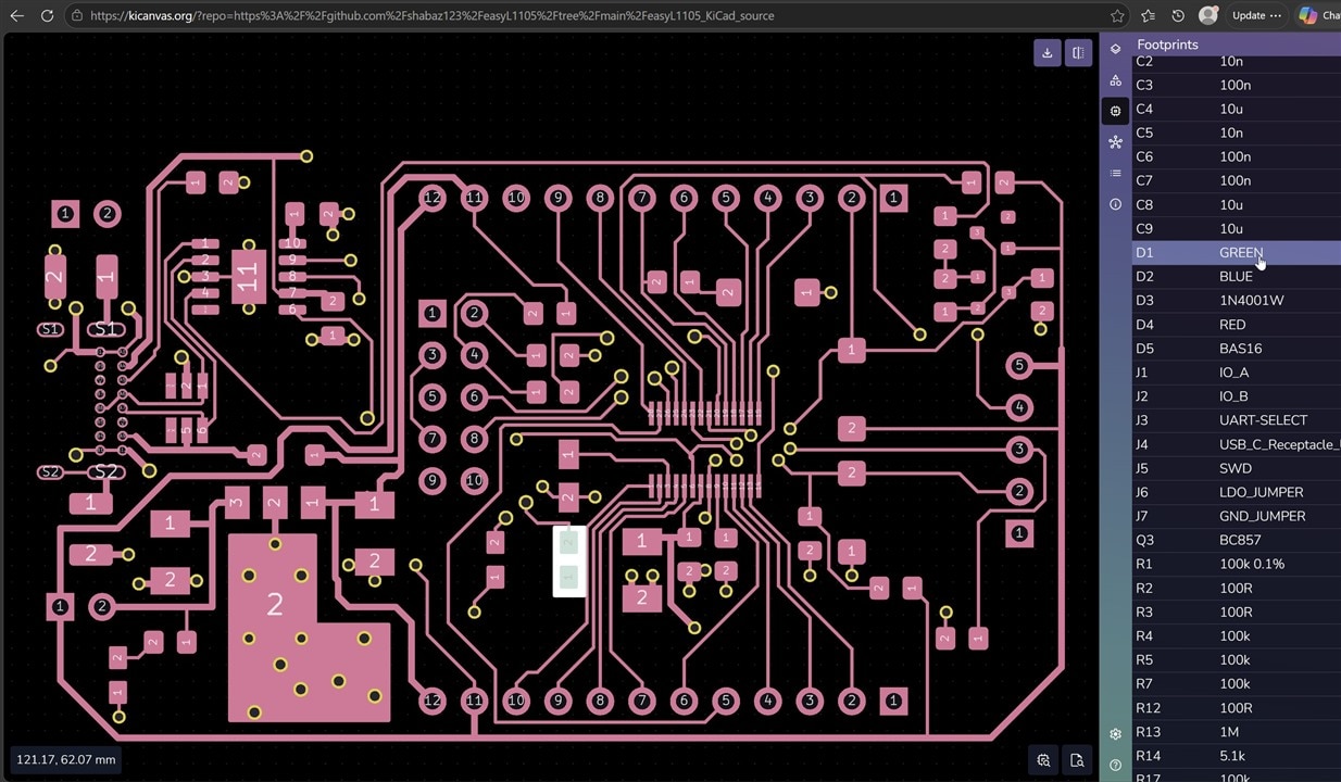
    The video didn't demonstrate much, but the ability to view and explore KiCad projects on desktop or mobile devices is already possible with KiCanvas (example PCB view).

    image

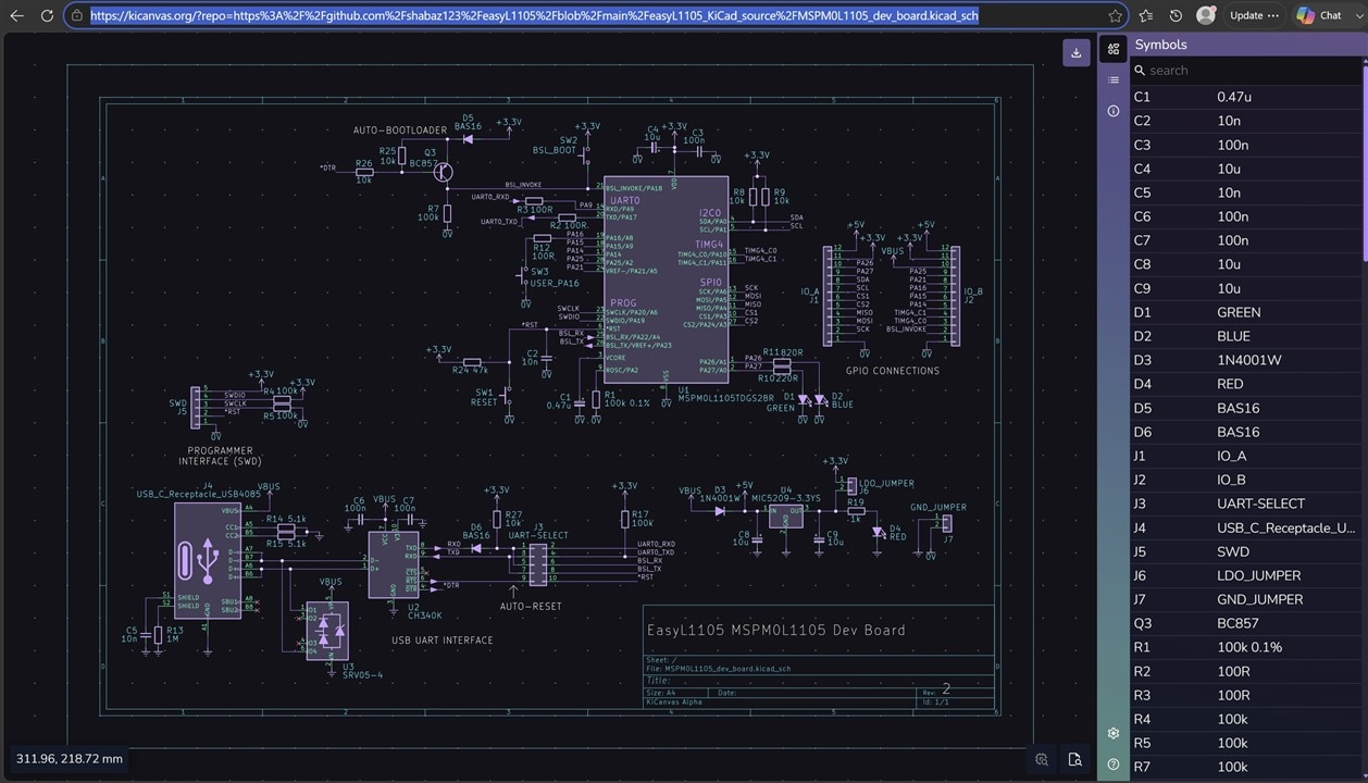
    Example schematic:

    image

    At least for hobbyists, that will go a long way toward reviewing, since third party tools can be used for capturing review meeting minutes and action items. That more informal method won't suit businesses of course.

    • Cancel
    • Vote Up +1 Vote Down
    • Sign in to reply
    • Cancel
  • BigG
    BigG 1 month ago in reply to shabaz

    Interesting, although it doesn't appear to be interactive like Altium365. I like to be able to click onto a component and it dynamically highlights the same component in different views (e.g. PCB, schematic, 3D view etc) and then provides you with the technical details (I found this option, at least in kicanvas).

    • Cancel
    • Vote Up +1 Vote Down
    • Sign in to reply
    • Cancel
>
element14 Community

element14 is the first online community specifically for engineers. Connect with your peers and get expert answers to your questions.

  • Members
  • Learn
  • Technologies
  • Challenges & Projects
  • Products
  • Store
  • About Us
  • Feedback & Support
  • FAQs
  • Terms of Use
  • Privacy Policy
  • Legal and Copyright Notices
  • Sitemap
  • Cookies

An Avnet Company © 2026 Premier Farnell Limited. All Rights Reserved.

Premier Farnell Ltd, registered in England and Wales (no 00876412), registered office: Farnell House, Forge Lane, Leeds LS12 2NE.

Follow element14

  • X
  • Facebook
  • linkedin
  • YouTube