RoadTest: Seeking an Electronics Engineer to Evaluate a Broadcom Optical Wireless Transceiver Kit
Author: yesha98
Creation date:
Evaluation Type: Evaluation Boards
Did you receive all parts the manufacturer stated would be included in the package?: True
What other parts do you consider comparable to this product?: None
What were the biggest problems encountered?: One of the key challenges encountered during evaluation was the absence of Broadcom-provided level conversion circuits or reference designs to translate LVDS/LVCMOS signals to the LVPECL interface required by the AFBR transceiver. This gap complicates system integration, as designers must develop and validate their own high-speed differential translation circuitry, increasing design time and risk of signal integrity issues. Providing official reference schematics, recommended translator ICs, and termination guidelines would greatly simplify adoption and ensure reliable electrical interfacing with Broadcom’s AFBR modules.
Detailed Review:
Introduction
The Broadcom AFBR-FS50B00 is a compact, high-speed optical wireless transceiver designed to enable full-duplex communication through free space at data rates up to 5 Gb/s over distances ranging from 30 mm to 100 mm.
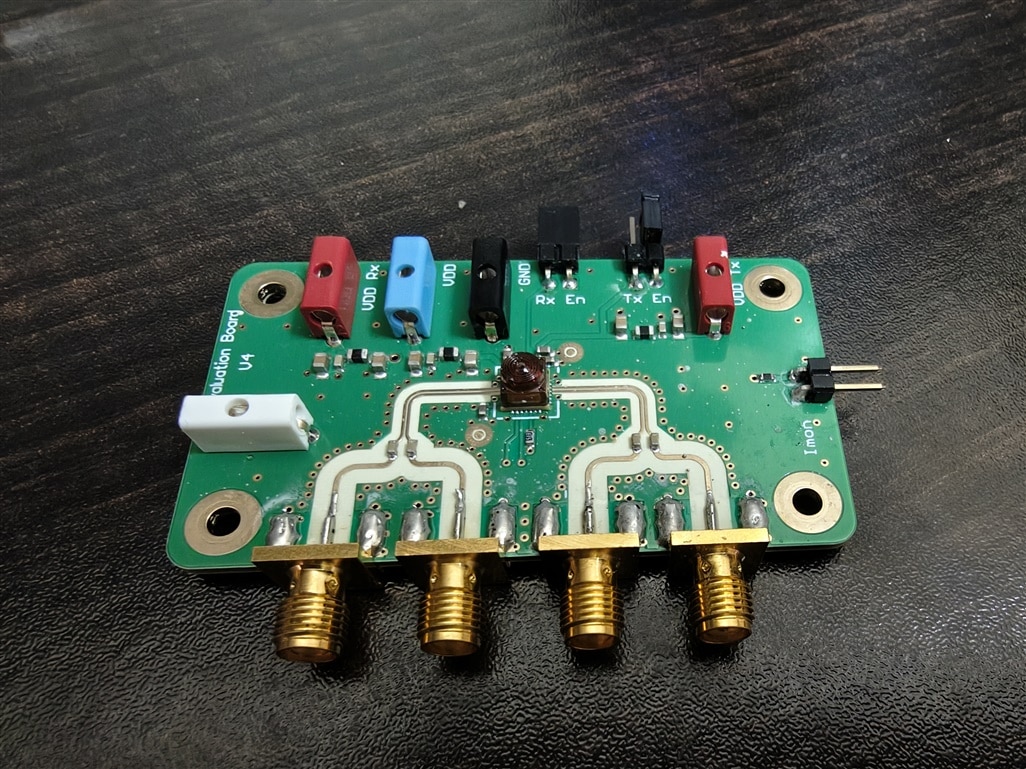
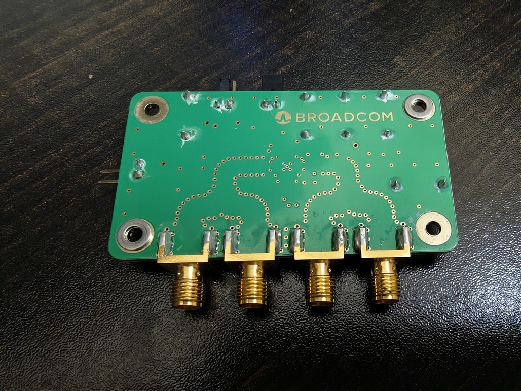
Unlike traditional fiber-based links, it transmits and receives data optically without physical connectors, making it ideal for board-to-board, rotary, and through-window communication where cabling or slip-rings are impractical. The device integrates an 850 nm VCSEL transmitter and a high-speed PIN photodiode receiver, both built into a small surface-mount package. It maintains full functionality across 360° rotation, offering excellent flexibility for compact system designs that require high-bandwidth, low-latency optical interconnects. To simplify evaluation, Broadcom provides the AFBR-FSEK50B00S evaluation kit, which includes two PCBs populated with AFBR-FS50B00 transceivers and SMA interfaces for signal input and output.
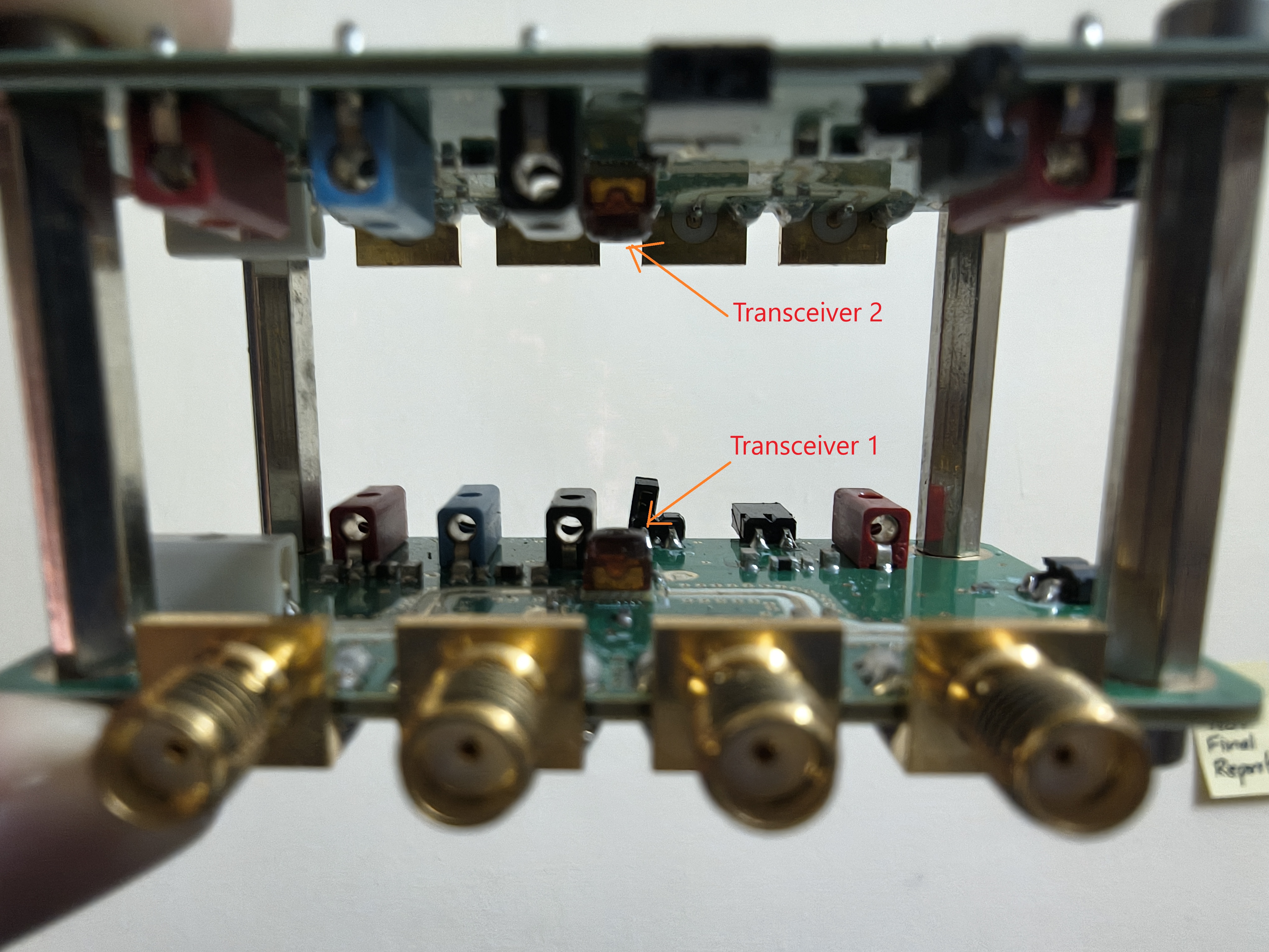
This setup allows designers to quickly validate optical link performance under real conditions, with verified error-free transmission demonstrated at 25 Mb/s, 1 Gb/s, and 5 Gb/s. The evaluation kit enables engineers to explore the transceiver’s capabilities in various applications, including industrial automation, automotive communication modules, and high-speed embedded systems. It provides an effective platform for studying optical alignment, signal integrity, and power optimization before integration into production hardware.
Objective
The primary objective of this experiment is to evaluate the performance and functionality of the custom-designed LVCMOS-to-LVPECL level conversion circuit intended for interfacing an FPGA with the Broadcom AFBR-FS50B00 optical transceiver. Specifically, the goal is to verify that the converter accurately translates the FPGA’s single-ended LVCMOS signals into differential, AC-coupled LVPECL signals with correct voltage swing, common-mode level, and transition integrity as required by the transceiver.
This phase focuses on observing and comparing the input and output waveforms using an oscilloscope and a logic analyzer to confirm proper signal translation, symmetry, and timing behavior. Successful validation of the converter’s operation ensures that the electrical interface to the AFBR transceiver will meet its input specifications and support stable high-speed optical communication in subsequent system-level testing.
System Overview
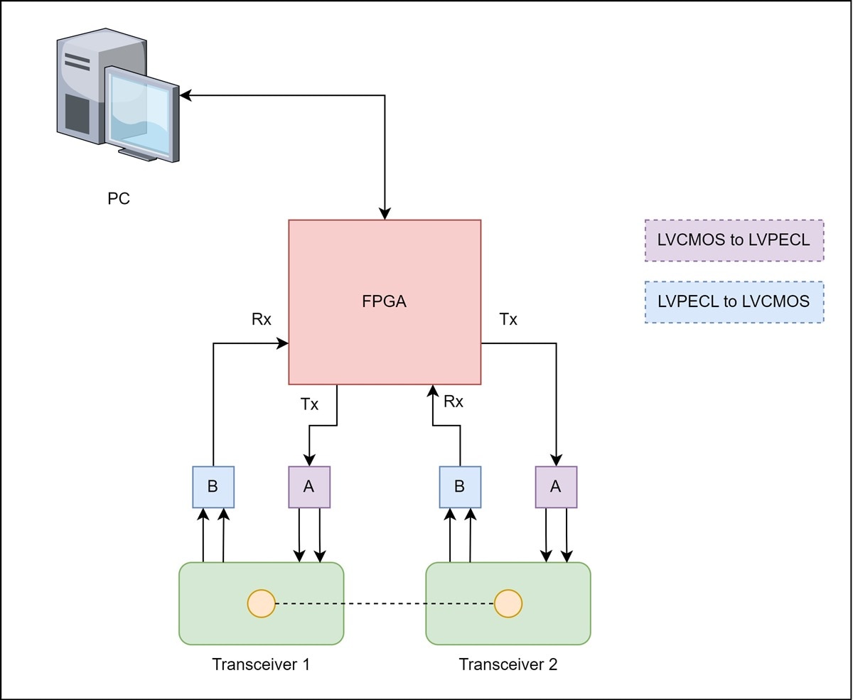
The experimental setup consists of an FPGA board, a custom-built LVCMOS-to-LVPECL level conversion circuit, and test instruments including an oscilloscope and a logic analyzer. The FPGA serves as the signal source, generating programmable LVCMOS outputs that emulate digital data streams intended for the Broadcom AFBR-FS50B00 optical transceiver. Since the transceiver’s input interface requires AC-coupled LVPECL differential signaling, the conversion circuit bridges the electrical compatibility gap between the two devices.
In this configuration, the FPGA outputs a defined logic pattern through its general-purpose I/O pins, which are routed to the input of the level-converter circuit. The converter translates the single-ended LVCMOS signals into differential LVPECL outputs, providing the appropriate voltage swing (~800 mVpp) and common-mode bias (~2 V) necessary for the AFBR-FS50B00. The differential outputs are AC-coupled to allow proper biasing and isolation between the converter and the transceiver input stage.
For validation, the LVCMOS inputs and LVPECL outputs are simultaneously monitored using an oscilloscope to capture the voltage waveforms and timing transitions, while the logic analyzer observes the digital characteristics of the LVCMOS signals. This setup allows direct comparison between input and output behavior, ensuring correct polarity, symmetry, and signal fidelity before integrating the converter with the optical transceiver module.
Circuit Design and Implementation
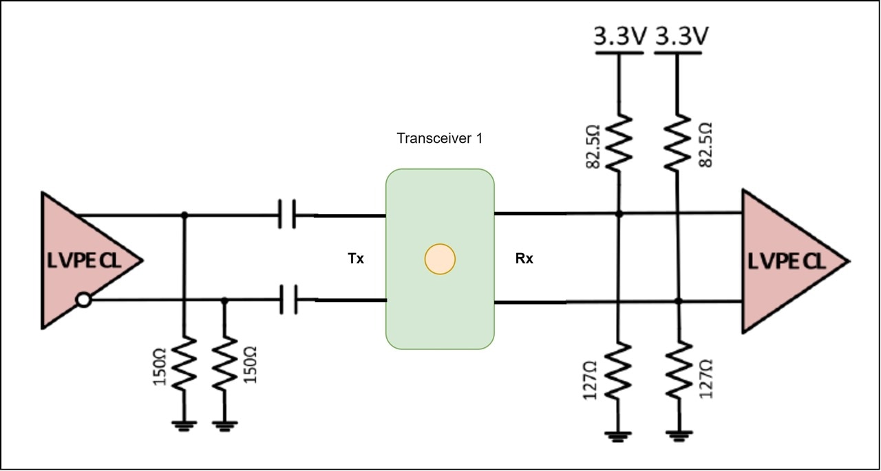
The interface circuit shown in figure implements an AC-coupled LVPECL link used to connect two Broadcom AFBR-FS50B00 optical transceivers (or, in this case, the FPGA-driven converter and a transceiver under test). The purpose of the design is to ensure proper biasing and signal integrity across the LVPECL differential lines while maintaining compatibility with the device’s required voltage levels and termination impedance.
Each LVPECL driver produces a differential output with a nominal common-mode voltage of about 2 V and a voltage swing of approximately 800 mV p-p. To block any DC bias mismatch between the driver and the receiver, the signals are AC-coupled using series capacitors placed on both the Tx and Rx differential pairs. The capacitors allow high-speed AC components to pass while isolating the DC bias networks on either side.
On the transmit side, 150 Ω pull-down resistors provide a defined DC reference to ground when the driver is AC-coupled, maintaining impedance matching and preventing floating nodes.
On the receive side, a resistor network consisting of 82.5 Ω pull-ups to 3.3 V and 127 Ω pull-downs to ground biases each differential line to the typical LVPECL common-mode voltage (~2 V). This passive bias network creates the proper DC level at the receiver input while maintaining an overall differential impedance close to 100 Ω, matching the transmission line and minimizing reflections.
The network therefore performs three key functions:
Provides the required biasing for LVPECL inputs through a resistive divider between 3.3 V and ground.
Ensures impedance matching along the entire high-speed path.
Maintains AC isolation between circuits, protecting against DC offset and allowing independent power-domain operation.
This configuration is particularly effective when interfacing devices with AC-coupled LVPECL I/O, such as the Broadcom AFBR-FS50B00 transceiver, ensuring stable high-speed operation without direct DC coupling between components. The design also facilitates easier signal observation at the Tx and Rx nodes, allowing verification of signal swing, common-mode voltage, and eye quality using an oscilloscope.

Prototype Assembly
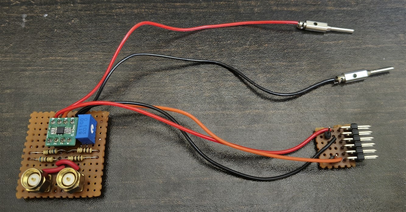
The prototype circuit was assembled on a perfboard to validate the operation of the LVCMOS-to-LVPECL level-conversion stage before integration with the Broadcom AFBR-FS50B00 transceiver. The design incorporates SMA connectors, banana jacks, and a PMOD-compatible header, allowing convenient interfacing with both laboratory instruments and the FPGA board.
The SMA connectors provide high-frequency signal access for the differential LVPECL outputs, enabling direct connection to an oscilloscope or a high-speed measurement setup with controlled impedance coaxial cables. The banana jacks supply regulated 3.3 V and ground connections to power the converter circuit, ensuring stable operation during signal testing. The PMOD interface is wired to the FPGA’s digital I/O pins, carrying the LVCMOS-level input signals into the converter stage. This arrangement allows the FPGA to act as the digital pattern generator while keeping the analog front-end isolated and easily accessible for probing.
The circuit employs precision resistors and coupling capacitors consistent with the schematic shown earlier, and a compact IC breakout board hosts the differential driver/translator device. The overall wiring layout minimizes loop area and parasitic capacitance, which is essential for preserving high-speed signal fidelity. This modular and manually soldered prototype provides a practical and flexible platform for real-time waveform observation, debugging, and validation of electrical level translation prior to full system integration with the optical transceiver.

Oscilloscope-Based Signal Integrity Verification

In addition to logic-level timing analysis, the converted LVPECL signals were examined using a high-bandwidth oscilloscope to evaluate analog signal integrity, biasing behavior, and edge characteristics. The figure on the left shows a dual-channel oscilloscope capture of the differential LVPECL waveform observed at the output of the level conversion circuit.
Channel 1 (yellow) and Channel 2 (green) correspond to the two complementary sides of the LVPECL differential pair. Both signals exhibit the expected out-of-phase behavior, confirming correct differential operation. The measured frequency of approximately 25 MHz matches the FPGA-generated input pattern, validating that the level conversion stage preserves timing and frequency accuracy.
AC-Coupling and Bias Network Behavior
The oscilloscope capture clearly illustrates the effect of AC coupling and passive bias restoration on the LVPECL signals. Rather than switching rail-to-rail, each differential line is biased around a mid-level voltage close to the expected LVPECL common-mode level (~2 V), as established by the resistor divider network on the receiver side.
The waveform shape shows a characteristic exponential settling following each transition, particularly evident during long runs of logic high or logic low. This behavior is a direct consequence of the AC-coupled architecture, where the coupling capacitors block DC content and the bias network re-establishes the operating point. Importantly, the observed baseline movement remains well within the LVPECL input tolerance and does not compromise logic interpretation.
The differential swing is consistent with LVPECL requirements, and no excessive overshoot, ringing, or reflection artifacts are visible. This confirms that the impedance matching provided by the termination network is effective and that the physical layout of the prototype does not introduce significant parasitic effects at the tested frequency.
Correlation with Logic Analyzer Timing Results
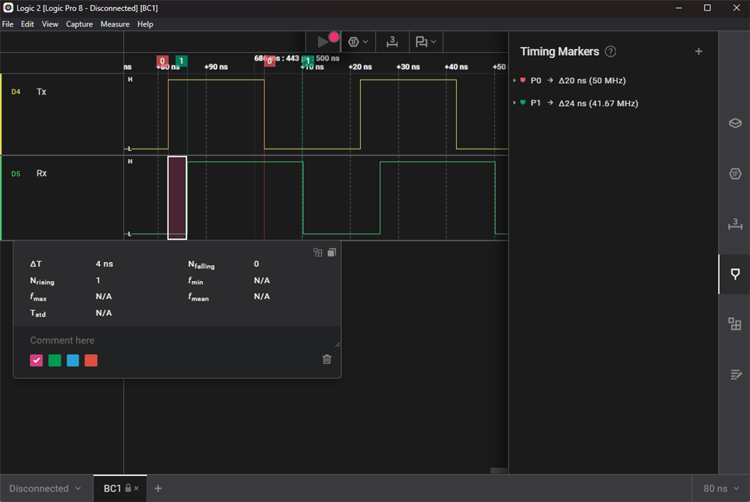
When correlated with the Saleae logic analyzer measurements, the oscilloscope data provides complementary insight into the system’s behavior. While the logic analyzer highlights the digital Tx-to-Rx delay of approximately 20–25 ns, the oscilloscope reveals the analog mechanisms contributing to this delay, including:
The slight asymmetry observed between rising and falling edges is consistent with the AC-coupled LVPECL interface and does not indicate any malfunction or instability. The delay remains deterministic and repeatable across cycles, which is critical for predictable system behavior.
End-to-End Electrical Confidence Before Optical Integration
Taken together, the oscilloscope and logic analyzer results confirm that the custom LVCMOS-to-LVPECL conversion circuit operates correctly both electrically and temporally. The converter produces clean, well-biased LVPECL signals with stable frequency and controlled edge behavior, while introducing only a small and predictable propagation delay.
This level of confidence in the electrical interface is essential before introducing the optical wireless link, as it ensures that any subsequent timing or integrity effects observed at the system level can be attributed to the transceiver or optical channel rather than the supporting interface circuitry.
Summary of Combined Measurements
No signal integrity issues such as ringing, metastability, or missing transitions
These results validate the readiness of the interface circuit for full integration with the Broadcom AFBR-FS50B00 optical transceiver and for subsequent higher-speed and system-level testing.
Results and Discussion
The custom LVCMOS-to-LVPECL level conversion circuit was successfully validated using both logic analyzer and oscilloscope measurements. The Saleae logic analyzer capture shows a clear and repeatable delay between the FPGA transmit (Tx) and receive (Rx) signals. The measured end-to-end Tx-to-Rx latency is approximately 20–25 ns, which remains consistent across multiple cycles, indicating deterministic system behavior.
Oscilloscope measurements of the LVPECL outputs confirm correct differential operation with the expected phase inversion between the complementary signals. The observed signal frequency (~25 MHz) matches the FPGA-generated input, demonstrating that the converter preserves timing accuracy. The AC-coupled interface establishes a stable LVPECL common-mode voltage through the passive bias network, with no significant overshoot, ringing, or reflection artifacts.
The slight edge asymmetry and baseline settling visible in the waveforms are consistent with AC-coupled LVPECL signaling and do not impact functional correctness. Overall, the results confirm that the level conversion circuit provides clean signal translation and predictable latency, making it suitable for reliable interfacing between the FPGA and the Broadcom AFBR-FS50B00 optical transceiver.


