RoadTest: Seeking more Engineers to Review a FRDM Development Board from NXP
Author: AngelSoto
Creation date:
Evaluation Type: Development Boards & Tools
Did you receive all parts the manufacturer stated would be included in the package?: True
What other parts do you consider comparable to this product?: Comparable products include development boards based on the Infineon PSoC and ESP32 families. Rather than performing a direct comparison, this RoadTest focused on evaluating the FRDM-MCXN947 on its own merits as an embedded development platform.
What were the biggest problems encountered?: No significant hardware or software issues were encountered during the evaluation. The board was operational immediately after unboxing, the MCU-Link debugger was detected automatically under Linux and the overall development workflow using MCUXpresso IDE was smooth. The main challenge was understanding the breadth of the MCUX SDK and identifying the most appropriate examples and software components for each experiment. Advanced features such as PowerQuad and the Neural Processing Unit are well documented, but fully understanding the complete software stack sometimes required consulting several documentation sources. During the customization of one SDK example, I also had to spend some time understanding how the board initialization, pin configuration and generated BSP files interacted. This was primarily a learning exercise rather than a limitation of the platform, but it illustrates the initial learning curve when moving beyond the supplied examples.
Detailed Review:
| Document Information | |
|---|---|
| Author | Ángel Soto Boullosa |
| Date | August 2026 |
| Revision | v1.0 |
A practical evaluation of the NXP FRDM MCX-N947 development board, covering the out-of-the-box experience, development workflow using MCUXpresso, hardware accelerators (PowerQuad and NPU), on-board peripherals and practical embedded applications.
The FRDM-MCXN947 is NXP's flagship development board for the MCX N94 and MCX N54 family of microcontrollers, designed to provide a compact yet powerful platform for rapid prototyping and embedded application development. Built around the high-performance MCX-N947 microcontroller, the board combines dual Arm Cortex-M33 cores running at up to 150 MHz with dedicated hardware accelerators, including the PowerQuad mathematical accelerator and a Neural Processing Unit (NPU), enabling applications that go well beyond traditional microcontroller workloads.
Beyond the processing capabilities of the MCU itself, the development board integrates many of the peripherals typically required during embedded development. These include an on-board MCU-Link debugger, USB Type-C connectivity, external flash memory, CAN-FD support, standard Arduino and mikroBUS expansion headers, an RGB user LED, user buttons, and a P3T1755 I3C/I²C temperature sensor. This combination allows the board to be evaluated immediately after unboxing while also providing an excellent platform for more advanced hardware and software experiments.
Unlike many traditional development boards that focus mainly on demonstrating basic peripheral functionality, the FRDM-MCXN947 highlights several of NXP's latest technologies, particularly hardware acceleration for mathematical processing and machine learning. These capabilities make the platform especially attractive for engineers working on digital signal processing, industrial control, edge AI, sensor fusion and other computationally intensive embedded applications.
The objective of this RoadTest is to perform a practical engineering evaluation of the NXP FRDM-MCXN947 development board, analysing not only its hardware capabilities but also the overall development experience offered by the NXP software ecosystem.
Rather than simply running the supplied examples, the evaluation follows a progressive approach that starts with the out-of-the-box experience and continues through development environment installation, software development, hardware accelerator benchmarking and implementation of a small real-world embedded application.
Particular attention is given to the technologies that distinguish the MCX-N947 from more conventional Cortex-M microcontrollers, namely the PowerQuad accelerator and the Neural Processing Unit (NPU). Their practical benefits will be investigated through dedicated experiments and compared against standard CPU execution whenever possible.
Finally, the review includes the implementation of a simple application using the on-board P3T1755 temperature sensor and RGB LED to demonstrate how the board can be used in a realistic embedded development workflow combining peripherals, firmware and user interaction.
The MCX family represents NXP's next generation of general-purpose microcontrollers, designed to provide higher performance, improved energy efficiency and enhanced security while maintaining the ease of use expected from modern embedded development platforms.
The portfolio spans multiple performance levels and application domains, allowing developers to select devices ranging from cost-optimised controllers to high-performance dual-core microcontrollers with integrated hardware accelerators. Across the family, NXP maintains a consistent software ecosystem based on MCUXpresso, helping developers migrate between devices while reusing drivers, middleware and development tools.
The MCX-N947 used in this evaluation belongs to the high-performance segment of the family and integrates features such as dual Arm Cortex-M33 cores, up to 2 MB of flash memory, hardware security features, external memory support and dedicated acceleration engines for mathematical processing and machine learning. These capabilities position the device as a compelling platform for applications requiring significantly more computational power than that offered by traditional microcontrollers.
This RoadTest focuses on evaluating the FRDM-MCXN947 from the perspective of an embedded software engineer. Rather than providing an exhaustive description of every peripheral available on the MCU, the review concentrates on the features that are likely to have the greatest impact on everyday development.
The evaluation covers the complete developer journey, including the initial unboxing experience, hardware inspection, installation of the MCUXpresso development environment, SDK exploration, project creation, programming and debugging workflow, and documentation quality.
Special emphasis is placed on experimentally evaluating the PowerQuad accelerator and the Neural Processing Unit through practical examples, followed by the implementation of a sensor-based demonstration using the on-board temperature sensor and RGB LED. Where appropriate, measurements, observations and engineering considerations are included to provide a realistic assessment of the platform's strengths and limitations.
The intention is not only to verify that the board functions as advertised, but also to determine how suitable it is for real embedded development projects, rapid prototyping and advanced applications involving digital signal processing, machine learning and intelligent sensing.
The first stage of this RoadTest focused on evaluating the initial user experience, from opening the package to powering up the board for the first time. A good development board should allow engineers to move quickly from unboxing to writing and testing code, while also providing clear documentation and a straightforward hardware setup.
This section documents the packaging, included accessories, first hardware inspection and the initial power-up experience using the factory-programmed firmware.
The FRDM-MCXN947 arrived in a compact cardboard package that protects the board well during shipping while keeping the presentation simple and professional. The packaging follows the familiar style used across NXP's FRDM family, providing a clean presentation without unnecessary accessories or excessive plastic.

Figure 1 : Front side of the FRDM-MCXN947 retail package
The front of the package clearly identifies the development board and highlights its main features. The rear side contains product identification labels, manufacturing information and additional markings that will be described in more detail once inspected.
The rear side of the package is intentionally simple and primarily contains product identification and regulatory information rather than marketing material. A large identification label provides the board type (FRDM-MCXN947), manufacturing and traceability information, including the product code, lot number, date code, serial identifiers and multiple barcodes and QR codes used for inventory and logistics.
The packaging also includes the expected regulatory markings (CE and UKCA), recycling information and NXP branding. While visually less informative than the front, the rear provides all the identification details typically expected for a professional development kit.

Figure 2 : Rear side of the FRDM-MCXN947 retail package
Inside the package the following items were included:

Figure 3 : Contents of the FRDM-MCXN947 evaluation kit
Although the kit contents are intentionally minimal, they include everything required to begin development immediately. No additional programmer or debug probe is required since the board integrates NXP's MCU-Link debugger.
The inclusion of a USB Type-C cable is a welcome detail, allowing the board to be connected directly to a development computer without requiring any additional accessories.
After removing the board from the packaging, the overall build quality makes a very good first impression. The PCB is well manufactured, with a clean silkscreen, clear component markings and an efficient layout that makes it easy to identify the main functional blocks.

Figure 4 : Hardware overview of the FRDM-MCXN947 development board
The top side of the PCB contains the MCX-N947 microcontroller together with the MCU-Link debugger, USB Type-C connectors, RGB LED, user buttons, the on-board P3T1755 temperature sensor and the main expansion interfaces.
An external serial Flash memory device (U8) is also populated on the board, located directly beneath the mikroBUS connector. This additional non-volatile memory extends the board's storage capabilities and can be used by applications requiring data storage beyond the MCU's internal Flash memory.

Figure 5 : Hardware overview of the FRDM-MCXN947 development board, rear view
The reverse side continues the clean layout, exposing additional routing while maintaining excellent manufacturing quality. Test points and reference labels are easy to identify, something that is always appreciated during debugging and hardware exploration.
One aspect that immediately stands out is the density of integrated peripherals. Despite the compact dimensions of the board, NXP has managed to integrate a large number of useful interfaces without making the layout appear crowded.
Before starting software development, it is worth taking a closer look at the main hardware features integrated on the board. The following annotated diagram, adapted from the official Quick Start Guide, provides a convenient overview of the most important components and expansion interfaces available on the FRDM-MCXN947.

Figure 6 : Overview of the main hardware features of the FRDM-MCXN947 development board (adapted from the Quick Start Guide)
As shown above, the board integrates considerably more than the target microcontroller itself. Alongside the MCX-N947 MCU, the development kit includes an on-board MCU-Link debugger, dual USB Type-C connectors, Ethernet connectivity, CAN-FD transceiver, Arduino-compatible headers, mikroBUS socket, PMOD connector, camera interface, FlexIO/LCD connector and several user peripherals, allowing many applications to be developed without requiring additional hardware.
Among the most relevant hardware features are:
The wide range of integrated peripherals and expansion interfaces reflects the board's focus on rapid prototyping. Most common embedded development scenarios can be explored directly on the evaluation board, while the available headers provide a straightforward path for connecting external hardware and developing more complex applications.
The first functional test consisted simply of connecting the board to a Linux development workstation using the supplied USB Type-C cable connected to the MCU-Link USB port.
The entire power-up sequence was recorded to document the board's behaviour straight out of the box.
Video 1 : First power-up of the FRDM-MCXN947 executing the factory-programmed firmware
Immediately after power-up, the board started executing the factory-programmed firmware without requiring any user interaction, confirming that the board was fully operational straight out of the box. The demonstration started automatically and provided an immediate indication that both the hardware and the factory firmware had been correctly programmed before shipment.
As part of the initial evaluation, it was also verified that the board was correctly detected by the host computer. No additional drivers or manual configuration were required under Linux, demonstrating that the integrated MCU-Link debugger is recognised automatically by the operating system.

Figure 7 : Linux kernel messages after connecting the FRDM-MCXN947
As shown in Figure 7, Linux successfully enumerated the board as an NXP MCU-Link CMSIS-DAP debug probe and automatically created a USB CDC ACM virtual serial port (ttyACM0). The operating system loaded the required HID and CDC drivers without requiring any additional software installation, confirming that the board was immediately ready for firmware development and debugging.
The detected USB descriptors identify the integrated debugger as MCU-LINK FRDM-MCXN947 (r0E7) CMSIS-DAP V3.128, providing both the CMSIS-DAP debug interface and a virtual serial port over a single USB connection.
At this stage only the basic hardware functionality and USB enumeration were verified. The complete development workflow, including MCUXpresso IDE installation, SDK configuration, project creation, firmware programming and debugging, will be covered in the next chapter.
Overall, the out-of-the-box experience was excellent. Within only a few minutes of opening the package, the board was powered, automatically recognised by the operating system and ready to begin software development, delivering exactly the rapid prototyping experience expected from a modern embedded development platform.
Before diving into software development and performance evaluation, it is worth taking a closer look at the hardware available on the FRDM-MCXN947. Although the board is compact, it integrates a surprisingly rich collection of peripherals and expansion options that make it suitable for both rapid prototyping and more advanced embedded development.
This chapter provides an overview of the most relevant hardware features that will be referenced throughout the remainder of this review.
At the heart of the board is the NXP MCX-N947, one of the most capable devices within the MCX family of microcontrollers. It combines two Arm Cortex-M33 cores running at up to 150 MHz with several hardware acceleration blocks that extend the computational capabilities far beyond those of a traditional microcontroller.
Among the most notable features are the integrated PowerQuad accelerator, intended for high-performance mathematical operations and digital signal processing, and the Neural Processing Unit (NPU), which enables efficient execution of TinyML inference workloads directly on the MCU.
The device also incorporates generous on-chip Flash and RAM resources, dedicated DMA engines, modern communication peripherals and advanced security features, making it suitable for applications ranging from industrial control to edge AI.

Figure 8 : Simplified block diagram of the FRDM-MCXN947 hardware architecture
The following architectural features are particularly relevant for this RoadTest:
Beyond the microcontroller itself, the FRDM-MCXN947 integrates a useful set of on-board peripherals that allow many experiments to be carried out without the need for additional hardware.
| Component | Purpose |
|---|---|
| MCU-Link | On-board programming and debugging interface |
| P3T1755 | Digital temperature sensor (I3C / I²C) |
| RGB LED | Visual status indication |
| User Buttons | User input and application control |
| Arduino Headers | Expansion interface compatible with Arduino shields |
| mikroBUS Connector | Support for MikroE Click Boards |
| CAN-FD Transceiver | CAN-FD communication experiments |
| USB Type-C Connectors |
Power, programming and USB communication |
| External Serial Flash (W25Q64JVSSIQ) |
Additional non-volatile storage for application data and firmware demonstrations. |

Figure 6 : Overview of the main hardware features of the FRDM-MCXN947 development board (adapted from the Quick Start Guide) (repeated for convenience)
The selection of integrated peripherals demonstrates that the board has been designed for practical embedded development rather than simply exposing the MCU pins. It integrates a comprehensive collection of peripherals and expansion interfaces, allowing many demonstrations and proof-of-concept applications to be developed without requiring additional external hardware.
One of the strengths of the FRDM platform is its flexibility. The board exposes a large portion of the MCU I/O through industry-standard expansion connectors, making it easy to prototype additional hardware without designing a custom PCB.

Figure 11 : Expansion connectors and prototyping interfaces of the FRDM-MCXN947
In addition to the Arduino UNO R3 compatible headers, the FRDM-MCXN947 also includes a mikroBUS socket, PMOD connector, FlexIO/LCD header and dedicated camera interface, providing compatibility with a wide range of existing expansion modules and rapid prototyping accessories.
These expansion options significantly extend the useful lifetime of the board, allowing it to evolve from simple demonstration projects to more complex embedded prototypes.
Good hardware is only part of the development experience. Equally important is the quality of the available documentation, development tools and software resources.
NXP provides an extensive documentation package for the MCX-N947 family, including a detailed Reference Manual, datasheet, User Manual, application notes and complete design files for the FRDM development board.
The documentation appears to be well organised and technically detailed, allowing developers to quickly locate register descriptions, peripheral information and hardware reference material when required.
Particularly valuable is the integration between the documentation and the MCUXpresso ecosystem, where software examples, SDK drivers and API documentation complement the hardware manuals.
The quality of the software ecosystem itself—including SDK organisation, example projects and IDE integration—will be evaluated in much greater detail during the following chapters once practical development begins.
| Document | Purpose |
|---|---|
| MCX-N947 Datasheet | Microcontroller specifications and peripheral capabilities. |
| FRDM-MCXN947 User Manual | Board overview, connectors, jumpers and hardware features. |
During the initial stages of this evaluation, these two documents were sufficient to understand the board architecture, identify the available peripherals and begin software development. Additional documentation, such as the Reference Manual, SDK documentation and application notes, will be consulted later as more advanced features, including PowerQuad, the NPU and other hardware accelerators, are explored.
A powerful development board also requires a mature software ecosystem. Modern embedded development depends not only on capable hardware, but also on a reliable IDE, a well-organised SDK, robust debugging tools and comprehensive documentation.
This chapter evaluates the complete setup process, from installing MCUXpresso IDE to compiling, programming and debugging the first application on the FRDM-MCXN947.
MCUXpresso IDE is NXP's Eclipse-based integrated development environment for its microcontroller portfolio. It integrates the GNU Arm toolchain, project management utilities, advanced debugging capabilities and seamless integration with the MCUXpresso SDK. The latest version of the IDE was downloaded directly from the NXP website, where several development tools are available depending on the target platform (Figure 12). For this evaluation, the Linux x86_64 installer was selected.
Installation on Ubuntu 24.04 LTS was straightforward. The provided installer automatically deployed not only the IDE itself, but also all the required development components, including LinkServer, the MCU-Link utilities, LPCScrypt and the SEGGER J-Link software package. During installation, the required udev rules were also configured, allowing supported USB debug probes to be accessed without requiring superuser privileges during normal development (Figure 13).
One small observation for Linux users is that the installer places the IDE under /usr/local/mcuxpressoide, but it does not automatically add the executable to the user's PATH. The IDE can be launched directly from its installation directory or by creating a launcher or updating the shell environment if command-line access is desired.
During the first launch, MCUXpresso prompted for a workspace location before opening the main development environment (Figure 14). No additional configuration was required, and the IDE was immediately ready for SDK installation and project development. Once the workspace had been created, the main window presented quick access to the most common development tasks, including SDK management, project creation and example import (Figure 15).
The evaluation was performed on Ubuntu 24.04 LTS using MCUXpresso IDE version 25.6.136.
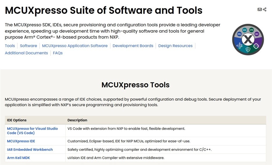
Figure 12: MCUXpresso IDE download page.

Figure 13: MCUXpresso IDE installation on Ubuntu Linux.

Figure 14: Workspace selection during the first launch of MCUXpresso IDE.

Figure 15: MCUXpresso IDE main window after installation.
Unlike some development environments where device support is bundled with the IDE, MCUXpresso separates the Integrated Development Environment from the Software Development Kit (SDK). This modular approach allows developers to install only the software packages required for the target board or MCU family, reducing unnecessary downloads and simplifying future updates.
SDK installation is fully integrated into MCUXpresso IDE. Selecting Download and Install SDKs opens the online SDK catalog, where all supported development boards and microcontrollers can be searched and filtered (Figure 16). During this evaluation, no user registration or login was required to access the SDK repository.

Figure 16 : MCUXpresso SDK Manager displaying the online SDK catalog.
The FRDM-MCXN947 development board was easily located through the integrated search function. The IDE identified the corresponding SDK package (SDK_2.x_FRDM-MCXN 26.6.000) together with the target device (MCXN947VDF) and the available Flash and RAM resources before installation (Figure 17).

Figure 17 : FRDM-MCXN947 SDK package selected for installation in MCUXpresso IDE.
Installing the SDK required only a single click. Once the download completed, MCUXpresso automatically associated the SDK with the current workspace, making the device immediately available for project creation and SDK example import. Reopening the SDK Manager confirmed that the package had been successfully installed and recognised by the IDE (Figure 18).

Figure 18: MCUXpresso IDE confirming that the FRDM-MCXN947 SDK is already installed and available for development.
The SDK package includes board support files, startup code, peripheral drivers, CMSIS support, middleware components, linker scripts and a comprehensive collection of example applications covering many of the MCU peripherals. This organisation allows developers to begin experimenting with the hardware almost immediately without creating projects from scratch.
Overall, the SDK installation process was quick, intuitive and fully integrated into the development environment. The entire procedure required no manual configuration beyond selecting the target board, allowing development to continue immediately after installation.
The FRDM-MCXN947 integrates an MCU-Link debug probe providing both CMSIS-DAP debugging and a USB virtual serial port through a single USB Type-C connection.
As already demonstrated during the initial power-up evaluation (see Figure 9), Linux automatically detected the integrated MCU-Link debugger and loaded the required USB HID and CDC ACM drivers without requiring any additional software installation or manual configuration.
Once the SDK had been installed, MCUXpresso IDE immediately recognised the available debug probe, allowing firmware download, debugging and serial communication to begin without any further setup.
This seamless integration between the operating system, the integrated debug probe and the development environment contributes significantly to the overall out-of-the-box experience, allowing developers to focus on application development rather than tool configuration.
To verify the complete software workflow, one of the SDK example applications was imported into the workspace using the integrated example importer provided by MCUXpresso IDE.
The process begins from the IDE welcome page by selecting Import SDK Examples, which launches the dedicated import wizard. After choosing Go straight to the Wizard, the IDE automatically detects the SDKs installed on the system and presents the list of supported development boards. Since only the FRDM-MCXN947 SDK had been installed during the previous step, the board was automatically available for selection without requiring any additional configuration.
After selecting the target board, MCUXpresso displays all the example applications included in the SDK, organised by category (drivers, demos, middleware, RTOS, Bluetooth, file systems and others), making it easy to locate demonstration projects for a particular peripheral or software component.
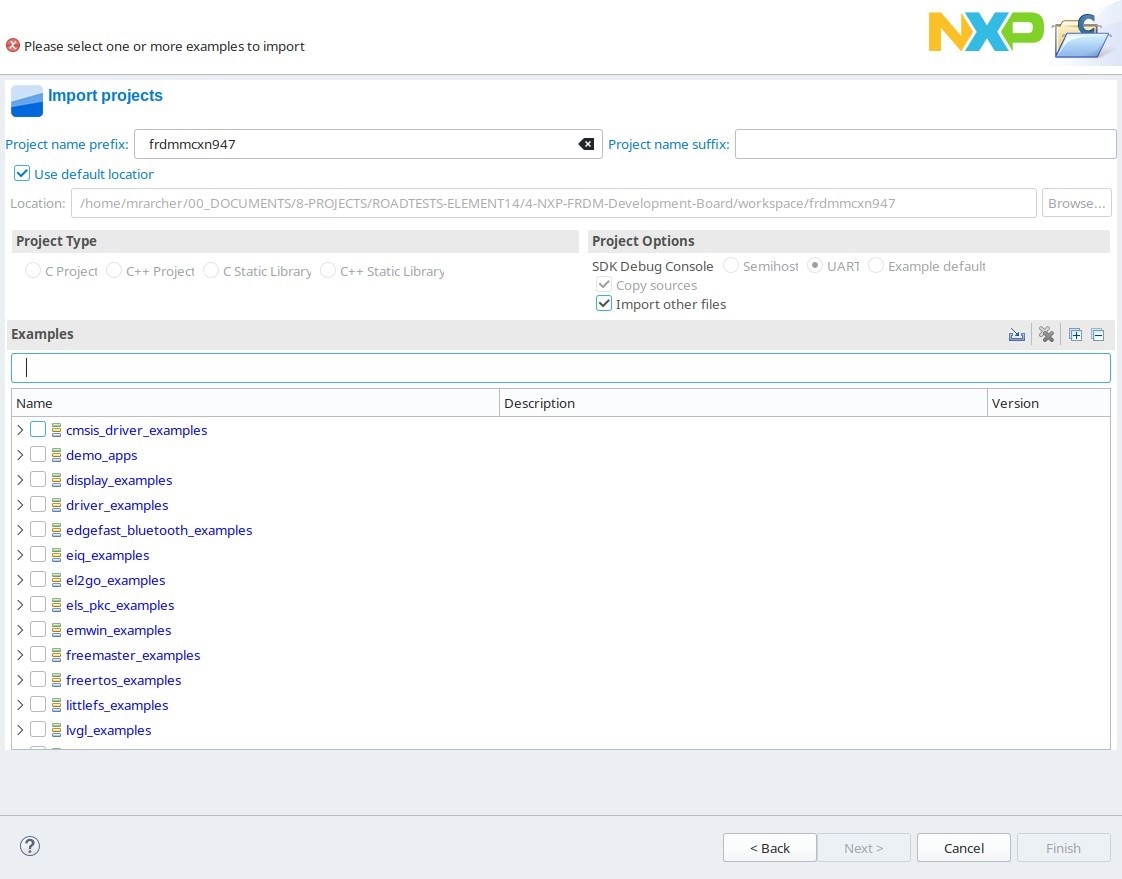
Figure 19 : SDK example projects available for the FRDM-MCXN947.
For the initial evaluation, the Hello World example was selected because it provides a quick end-to-end verification of the complete development workflow while keeping the application itself intentionally simple.
During project creation, the IDE presented the default project configuration, including the runtime library, compiler settings, memory layout and debug console options. For this evaluation, the default settings generated by the SDK were kept unchanged, with the exception of redirecting the SDK debug console to the UART interface in order to simplify verification through the virtual COM port exposed by the on-board MCU-Link debugger.

Figure 20 : Importing the Hello World example into the workspace.
Once the wizard completed, MCUXpresso automatically generated the complete project structure, including the startup code, linker scripts, board support package, peripheral drivers and source files required by the example. The project appeared immediately in the Project Explorer and was ready to be compiled without any additional manual configuration.

Figure 21 : Hello World example imported successfully into the MCUXpresso workspace.
Once imported into the workspace, the project was compiled without requiring any modifications to the source code. This verified that the SDK, GNU Arm toolchain and project configuration were correctly integrated and ready for immediate development.
The project was built directly from within MCUXpresso IDE using the default Build Project command. The IDE automatically invoked the GNU Arm Embedded toolchain, generated all intermediate object files and produced the executable image together with the corresponding ELF and MAP files.

Figure 22 : Successful build of the Hello World example showing memory usage and compilation summary.
The compilation completed successfully in 1.91 seconds, producing no errors or warnings. The generated executable occupied 15.0 kB of Flash (1.43%) and 8.7 kB of SRAM (2.22%), confirming that the SDK example builds correctly without requiring any manual configuration of compiler options, linker scripts or include paths.
The integrated memory usage report provides an immediate overview of Flash and RAM consumption after every build. As expected for a simple Hello World application, the generated firmware occupies only a small fraction of the available on-chip memory, leaving ample resources for more complex applications.
This successful build confirmed that the complete software toolchain, from project generation through compilation and linking, was fully operational before proceeding to firmware programming and debugging.
Programming the firmware was performed directly from within MCUXpresso IDE using the integrated MCU-Link CMSIS-DAP debug probe supplied with the FRDM-MCXN947 development board. No external programmer, additional drivers or third-party flashing utilities were required.
After successfully compiling the project, the programming sequence was initiated by selecting Run -> Debug As -> MCUXpresso IDE LinkServer (CMSIS-DAP) probes, which launches the integrated LinkServer debugger provided by NXP.

Figure 23: Starting a debug session using the integrated MCU-Link LinkServer interface.
On the first execution, MCUXpresso automatically detected the on-board MCU-Link probe connected through USB and presented it for selection. Since only a single probe was connected to the host computer, no additional configuration was necessary.

Figure 24: Automatic detection of the integrated MCU-Link CMSIS-DAP debug probe.
Before programming the target, the IDE displayed a warning indicating that the imported project targets the MCXN947 device family, while the connected board identifies itself as the MCXN947VDFT package variant. This proved to be only an informational warning related to the exact package variant, as the firmware programmed and executed correctly without requiring any project modifications.

Figure 25: Device package compatibility warning shown before programming the target MCU.
MCUXpresso then detected the two Cortex-M33 cores available in the MCU and requested the target core to be selected before establishing the debug session. Once confirmed, the IDE automatically erased the internal Flash memory, downloaded the application, verified the programmed image and started the debugging session.

Figure 26: Selecting the Cortex-M33 target core before establishing the debug session.
The entire programming process completed successfully on the first attempt. During the evaluation, no communication failures, programming errors or unexpected disconnects were observed.
One of the strongest aspects of the FRDM platform is the seamless integration between the hardware and the software tools. Programming, debugging and virtual serial communication all operate through the same USB connection, considerably simplifying the initial development workflow and reducing the amount of external hardware required.
Overall, firmware download proved to be both fast and reliable, allowing new firmware revisions to be programmed within only a few seconds during normal development iterations.
After programming the firmware, MCUXpresso automatically entered the debug perspective and halted execution at the beginning of the application's main() function before executing any user code. This behaviour allows the application to be inspected immediately after reset without requiring manual breakpoint configuration.

Figure 27: Initial debug session with execution halted at the entry of the main() function.
The integrated debugger provides direct access to the processor registers, global and local variables, peripheral register views, memory usage information and source-level debugging. During the evaluation all these views updated correctly while stepping through the application.
Single-step execution was evaluated using the Step Over command. The debugger advanced through the initialization code exactly as expected while continuously updating register values and the current program counter.

Figure 28: Executing the application instruction-by-instruction using the Step Over command.
Breakpoint handling also operated reliably. After resuming program execution, the debugger stopped immediately at a user-defined breakpoint placed on the second PRINTF() instruction, demonstrating correct breakpoint insertion and execution control (Figure 29).

Figure 29: Execution stopped at a user-defined breakpoint during program execution.
Finally, after resuming execution, the application continued normally and produced the expected output through the integrated USB virtual serial port. The terminal displayed both the SDK version and the Hello World message generated by the example application, confirming that the UART debug console configured during project import was functioning correctly.

Figure 30: UART terminal showing the successful execution of the Hello World example.
Throughout the evaluation, debugging remained responsive and stable. Breakpoints, single-stepping, register inspection, peripheral inspection and serial output all worked correctly without communication issues or unexpected debugger disconnects.
The integrated MCU-Link probe, together with LinkServer and MCUXpresso IDE, provides a polished development experience that requires virtually no manual configuration, allowing developers to move from compiling firmware to full source-level debugging within only a few clicks.
The following table summarises the time required to complete each stage of the initial development environment setup. Although the exact duration depends on the host computer and internet connection, it provides a realistic indication of how quickly a developer can progress from downloading the development tools to executing and debugging the first application.
| Step | Description | Elapsed Time | Notes |
|---|---|---|---|
| Download MCUXpresso IDE | Download the installer from NXP | ~2 min | Depends on internet connection |
| Install MCUXpresso IDE | Complete IDE installation | ~3 min | Default installation options |
| Download SDK | Install the FRDM-MCXN947 SDK package | ~2 min | Installed directly through the integrated SDK Manager |
| Launch IDE | First startup and workspace creation | ~1 min | Workspace selection and initial indexing |
| Import Example Project | Import the Hello World SDK example | ~2 min | Automatic project generation |
| First Build | Compile the project successfully | ~1.91 s | No errors or warnings |
| Flash Firmware | Program the MCU through MCU-Link | ~3 s | Automatic erase, download and verification |
| Start Debug Session | Connect debugger and halt execution | ~3 s | Automatic breakpoint at main() |
| Total Time | From IDE download to the first debug session | ~10–12 min | Excluding user reading time and download speed variations |
| Additional Software Required | Extra packages installed outside MCUXpresso | N/A | No additional software or drivers were required. |
Overall, the software setup experience proved to be one of the strongest aspects of the FRDM-MCXN947 platform. From downloading MCUXpresso IDE to programming and debugging the first application, the complete workflow required only a few straightforward steps and virtually no manual configuration.
The automatic SDK management, integrated project templates, built-in LinkServer debugger and on-board MCU-Link probe provide a highly streamlined development experience. Project creation, compilation, programming, debugging and UART communication are all available directly from within the IDE, allowing development to begin within only a few minutes.
During the evaluation, breakpoint insertion was immediate and source-level debugging remained responsive throughout multiple programming cycles. Register inspection, peripheral register visualization, variable monitoring and memory usage views all operated correctly without requiring additional configuration.
Live variable inspection functioned as expected while execution was halted at breakpoints. Hello World example relied exclusively on the integrated UART virtual COM port for console output.
The only minor issue encountered during the evaluation was an informational warning indicating that the imported project targeted the MCXN947 device family while the evaluation board reported the MCXN947VDFT package variant. This warning did not affect programming or debugging, and the example executed correctly without requiring any project modifications.
Overall, the software ecosystem provided by NXP is polished, well integrated and beginner-friendly while still exposing the advanced debugging capabilities expected by experienced embedded developers.
Once the development environment had been successfully configured and the first example project compiled, the next step was to explore the MCUXpresso SDK supplied for the FRDM-MCXN947.
For most embedded projects, the SDK represents the starting point of every application. Beyond providing peripheral drivers, it also includes board support packages, middleware components, startup code and a large collection of reference examples. Consequently, the quality and organisation of the SDK have a significant impact on developer productivity.
Rather than reviewing every software component individually, this chapter focuses on the aspects that are most relevant during day-to-day embedded development: project organisation, discoverability of drivers and examples, documentation quality and overall usability.
The MCUXpresso SDK follows a structured directory layout that clearly separates the different software layers required to develop an embedded application.

Figure 31 : Project structure of the imported MCUXpresso SDK project showing the main software components.
At the highest level, the project contains dedicated folders for board support files, peripheral drivers, device-specific startup code, middleware components and user application sources. This separation makes it relatively easy to distinguish between vendor-supplied code and application-specific files.
During the evaluation, the folders most frequently accessed were:
After only a short period of exploration, navigating through the project became straightforward. The naming convention used throughout the SDK is consistent, making it easy to locate the files associated with a particular peripheral or board feature.
One of the strengths of the SDK is the comprehensive collection of peripheral drivers provided for the MCX-N947.
Although direct register access remains possible, the SDK provides high-level peripheral drivers that simplify hardware configuration while preserving access to low-level functionality whenever required.
Throughout this RoadTest several drivers will be used directly, including:
The naming convention adopted by NXP is consistent across the SDK, with driver files following the fsl_ prefix. This makes locating APIs relatively intuitive even before consulting the documentation.
A particularly valuable part of the SDK is the extensive collection of ready-to-build example projects.

Figure 32 : SDK Example Import Wizard listing the software examples available for the FRDM-MCXN947.
Rather than providing isolated code fragments, the examples are complete applications that can be imported directly into the IDE and executed with minimal effort.
The examples are grouped according to functionality, covering topics such as:
This organisation significantly reduces the time required to evaluate individual peripherals, since working reference implementations are already available.
Several of the examples evaluated during this RoadTest form the basis of the practical experiments presented in the following chapters.
Rather than starting from an empty project, most experiments presented later in this RoadTest were built by extending existing SDK examples. This considerably reduced development time and allowed the focus to remain on evaluating the hardware rather than configuring the software infrastructure.
Beyond the software itself, the accompanying documentation proved to be equally important.
The SDK integrates closely with the MCUXpresso IDE, allowing projects to be imported and built without requiring manual configuration of compiler options or linker scripts. API names are generally descriptive and the project structure is sufficiently clear that many files can be understood without constantly referring to the Reference Manual.

Figure 33 : Example of an SDK driver API integrated into the development environment.
Whenever additional information was required, the SDK documentation, User Manual and Reference Manual complemented each other well, providing enough information to understand both the software architecture and the underlying hardware.
During the evaluation it was rarely necessary to inspect the startup code or linker configuration manually, as the supplied examples already provided correctly configured projects for the development board.
One positive aspect observed throughout the evaluation was that the supplied examples were not merely demonstration programs but realistic starting points for custom developments.
From a software engineering perspective, the MCUXpresso SDK appears mature and well maintained. The consistent directory structure, extensive example collection and close IDE integration contribute to a development workflow that allows engineers to become productive very quickly.
The project organisation is logical, the driver libraries follow a consistent structure and the supplied examples considerably reduce the effort required to begin developing applications for the MCX-N947.
Rather than forcing developers to build projects from scratch, the SDK encourages an incremental workflow in which existing examples can be adapted to implement new functionality. This approach proved particularly useful during this RoadTest, where the same software infrastructure was progressively extended to evaluate the PowerQuad accelerator, the Neural Processing Unit and the on-board peripherals.
Overall, the SDK appears mature, well organised and closely integrated with the development tools, providing a solid software foundation for both evaluation and professional embedded development.
Arguably the most distinctive feature of the MCX-N947 is the inclusion of the PowerQuad hardware accelerator. Unlike a conventional Cortex-M microcontroller, where mathematical operations are executed exclusively by the CPU, the MCX-N947 integrates dedicated hardware capable of accelerating a wide range of Digital Signal Processing (DSP) operations.
The PowerQuad engine targets applications such as motor control, sensor fusion, audio processing, industrial control and other workloads where mathematical performance is critical. By offloading computationally intensive algorithms from the Cortex-M33 core, the accelerator can significantly reduce execution time while leaving the CPU available for other application tasks.
One of the objectives defined in the RoadTest Test Plan was to evaluate the practical benefits of this hardware accelerator. Rather than relying solely on the published specifications, this chapter evaluates the PowerQuad using the official MCUXpresso SDK examples and compares its performance against equivalent CMSIS-DSP software implementations running on the Cortex-M33 CPU.
Before performing any measurements, the first step consisted of exploring the PowerQuad examples included within the MCUXpresso SDK.

Figure 34: PowerQuad example projects available in the MCUXpresso SDK.
The SDK provides a comprehensive collection of example applications covering multiple aspects of the hardware accelerator. Examples are available for mathematical functions, matrix operations, FIR filters, FFT processing, vector operations and benchmarking. In addition to demonstrating the API, several examples directly compare the performance of the hardware accelerator against the equivalent CMSIS-DSP software implementation.
This approach proved particularly useful because it allowed the evaluation to build upon well-tested reference applications supplied by NXP rather than developing synthetic benchmarks from scratch.
Among the available projects, three examples were selected for further evaluation:
These projects provide an excellent basis for comparing hardware acceleration with conventional CPU execution under identical conditions.
The first example executed during the evaluation was the powerquad_math demonstration supplied with the SDK.

Figure 35: Imported PowerQuad example project within MCUXpresso IDE.
The project imports directly into MCUXpresso IDE without requiring any manual configuration. As with the previous SDK examples, the project structure clearly separates board support files, startup code, drivers and application sources, making navigation straightforward.
The application entry point initialises the development board, configures the debug console and enables the PowerQuad peripheral and then sequentially executes a large collection of mathematical demonstration functions.

Figure 36: Main application flow of the PowerQuad mathematical example.
Rather than implementing a single benchmark, the application exercises a broad selection of mathematical functions including logarithms, inverse functions, square roots, exponential functions, trigonometric operations and vector processing.
Each function validates the hardware-generated result against a reference software implementation to verify correctness before continuing with the next test. This verification ensures that the accelerator not only improves execution speed but also produces numerically equivalent results.

Figure 37: Floating-point square root example implemented using the PowerQuad API.
The software itself remains remarkably compact. From the application developer's perspective, using the accelerator primarily consists of initialising the peripheral through the SDK and invoking the appropriate PowerQuad API functions. Much of the low-level hardware configuration is abstracted by the driver library, allowing developers to concentrate on the algorithm rather than peripheral management.
After compilation, the project built successfully without requiring any modifications.

Figure 38: Successful compilation of the PowerQuad mathematical example.
Executing the application produced the expected UART output confirming that every mathematical test completed successfully.

Figure 39: UART output confirming successful execution of the PowerQuad mathematical example.
This initial experiment demonstrated that integrating the accelerator into an application requires relatively little software effort while providing immediate access to a rich collection of hardware-accelerated mathematical functions.
Once the basic functionality had been verified, the evaluation proceeded to the benchmark applications supplied by the SDK.
Rather than developing custom timing code, the official benchmark projects were executed to compare identical mathematical operations using two different execution paths:
Both benchmark applications execute the same collection of mathematical functions repeatedly while measuring the total execution time using the timing facilities provided by the SDK. The only difference between the two applications is the execution backend: one relies exclusively on CMSIS-DSP software routines, while the other redirects the same operations to the PowerQuad hardware accelerator.
The benchmark includes representative DSP-oriented operations such as:
Note: The suffixes Q15 and Q31 refer to fixed-point numerical formats using 16-bit and 32-bit signed integers respectively, while f32 denotes standard 32-bit IEEE-754 floating-point arithmetic. These formats are widely used in DSP applications to balance precision, execution speed and memory footprint.
Each benchmark function was executed 100,000 iterations, ensuring that the measured execution time is sufficiently large to minimise measurement noise while remaining representative of typical embedded workloads.
The PowerQuad benchmark project compiled successfully without modification.

Figure 40: Successful compilation of the PowerQuad benchmark application.
Running the benchmark produced the execution times shown below.

Figure 41: UART output of the PowerQuad benchmark application.
The equivalent software-only benchmark was then compiled and executed under the same conditions.

Figure 42: Successful compilation of the software benchmark application.

Figure 43: UART output of the Cortex-M33 software benchmark.
The measured execution times are summarised below.
| Benchmark Function | Software (CPU) | PowerQuad | Speed-up | Comments |
|---|---|---|---|---|
| arm_sqrt_q15 | 55 ms | 20 ms | 2.75× | Significant improvement for fixed-point square root. |
| arm_sqrt_q31 | 91 ms | 20 ms | 4.55× | Largest performance gain observed. |
| arm_sin_q15 | 21 ms | 17 ms | 1.24× | Moderate acceleration. |
| arm_sin_q31 | 26 ms | 17 ms | 1.53× | Noticeable performance improvement. |
| arm_sin_f32 | 33 ms | 16 ms | 2.06× | Floating-point operation benefits considerably. |
| arm_cos_q15 | 24 ms | 17 ms | 1.41× | Moderate improvement. |
| arm_cos_q31 | 27 ms | 17 ms | 1.59× | Consistent acceleration. |
| arm_cos_f32 | 35 ms | 16 ms | 2.19× | Strong improvement for floating-point cosine. |

Figure 44: Execution time comparison between the Cortex-M33 software implementation and the PowerQuad hardware accelerator for representative CMSIS-DSP mathematical functions. Lower execution times indicate better performance.
The results clearly demonstrate that the PowerQuad hardware accelerator provides measurable performance improvements across all evaluated mathematical functions.
The largest improvement was observed for the Q31 square root implementation, where execution time decreased from 91 ms to 20 ms, representing a speed-up of approximately 4.5×. Floating-point trigonometric functions also benefited significantly from hardware acceleration, while simpler fixed-point sine and cosine operations exhibited more modest but still measurable gains. Although the performance gain varies depending on the mathematical operation, every benchmark executed faster when using the PowerQuad accelerator.
These results confirm that the PowerQuad is particularly beneficial for computationally intensive DSP workloads where mathematical throughput is an important design constraint.
From a software engineering perspective, the PowerQuad proved straightforward to evaluate using the MCUXpresso SDK.
The supplied examples are well organised, compile without modification and provide both functional demonstrations and realistic performance benchmarks. The SDK abstracts most of the hardware-specific configuration behind a consistent API, allowing developers to integrate hardware acceleration with relatively little additional code.
The benchmark results obtained during this RoadTest confirm that the accelerator is capable of providing substantial performance improvements for several commonly used DSP functions while maintaining a simple programming model.
Overall, the PowerQuad represents one of the most compelling features of the MCX-N947 platform. Rather than being a specialised peripheral with limited practical value, it integrates naturally into the software ecosystem provided by the SDK and offers tangible performance benefits that can be exploited in real embedded applications. The benchmark results obtained during this evaluation demonstrate that the performance improvements are not merely theoretical but can be observed directly using the official SDK examples provided by NXP.
In addition to the PowerQuad mathematical accelerator evaluated in the previous chapter, the MCX-N947 also integrates a dedicated Neural Processing Unit (NPU). While the PowerQuad is intended to accelerate Digital Signal Processing (DSP) algorithms, the NPU targets a different class of workloads: machine learning inference.
The integration of dedicated AI hardware is one of the distinguishing characteristics of the MCX-N947 family and reflects the growing adoption of Edge AI, where intelligent decisions are performed directly on the embedded device without relying on cloud connectivity.
One of the objectives defined in the original RoadTest Test Plan was to evaluate the TinyML capabilities of the platform by deploying a small neural network model, executing inference on the target MCU and analysing both the software workflow and the runtime performance.
Rather than developing a custom neural network from scratch, this evaluation focuses on the official TensorFlow Lite Micro examples supplied within the MCUXpresso SDK. Using the vendor-provided examples ensures that the hardware is exercised using the software stack recommended by NXP while simultaneously providing a realistic overview of the developer experience.
Before executing any neural network, the first step consisted of exploring the machine learning examples included within the MCUXpresso SDK.

Figure 45: TensorFlow Lite Micro (TinyML) example projects available in the MCUXpresso SDK.
Unlike previous generations of Cortex-M microcontrollers, the SDK already includes a dedicated set of Embedded Intelligence (eIQ) examples based on TensorFlow Lite Micro. Several demonstration applications are provided, including image classification, keyword spotting and model runner examples.
Among the available projects were:
These examples demonstrate that machine learning is considered a first-class capability of the software ecosystem rather than an optional middleware component.
For this RoadTest, the TensorFlow Lite Micro CIFAR-10 example was selected because it provides a complete end-to-end TinyML application while exercising the dedicated Neural Processing Unit integrated into the MCX-N947.
Although TinyML and the Neural Processing Unit are often mentioned together, they represent different parts of the software stack.
TinyML refers to the execution of machine learning models on resource-constrained embedded systems. In this SDK, TinyML applications are implemented using TensorFlow Lite Micro, Google's lightweight inference framework designed specifically for microcontrollers.
TensorFlow Lite Micro provides the runtime responsible for loading the neural network, managing tensors and executing inference. The Neural Processing Unit, on the other hand, accelerates only those operations that have been mapped onto dedicated hardware.
Unlike a conventional software implementation where every neural network layer executes on the Cortex-M33 CPU, TensorFlow Lite Micro dispatches supported operations to the NPU while unsupported operators continue to execute on the processor. From the application developer's perspective, both execution paths are managed transparently by the TensorFlow Lite Micro interpreter.
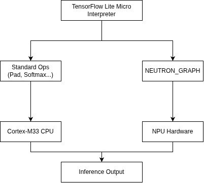
Figure 46: Software architecture showing how TensorFlow Lite Micro dispatches supported operations to the Neural Processing Unit while standard operators continue to execute on the Cortex-M33 CPU.
This hybrid execution model allows hardware acceleration to be introduced without fundamentally changing the application structure. Developers continue working with the TensorFlow Lite Micro API while the SDK automatically routes supported operators towards the dedicated hardware accelerator.
One particularly interesting implementation detail became apparent after examining the SDK source code. The application itself contains very little NPU-specific code. Instead, TensorFlow Lite Micro registers a custom operator called NEUTRON_GRAPH, representing the portion of the neural network that executes on the hardware accelerator.

Figure 47: TensorFlow Lite Micro operator resolver registering both standard TensorFlow Lite operators and the NPU-specific NEUTRON_GRAPH custom operator.
Besides the custom NPU operator, standard TensorFlow Lite operators such as Pad, Softmax and Dequantize continue to execute through the normal TensorFlow Lite runtime. This illustrates how NXP integrates the NPU into the standard TensorFlow Lite Micro execution model instead of requiring developers to implement a separate inference engine.
The selected CIFAR-10 example imports directly into MCUXpresso IDE without requiring any manual configuration.

Figure 48: Imported TensorFlow Lite Micro CIFAR-10 project inside MCUXpresso IDE.
The project organisation follows the same conventions observed throughout the SDK. Board support files, startup code, peripheral drivers and application sources are clearly separated, while additional folders contain the TensorFlow Lite Micro runtime and the embedded machine learning model.
The application entry point is intentionally compact.

Figure 49: Main application flow of the TensorFlow Lite Micro CIFAR-10 example.
After initialising the hardware platform, the application performs the following sequence:
The overall application structure remains remarkably simple. Most of the machine learning complexity is encapsulated inside the TensorFlow Lite Micro runtime, leaving the application responsible only for supplying the input data and consuming the inference results.
Model initialisation is equally straightforward.

Figure 50: TensorFlow Lite Micro model initialisation showing model loading, interpreter creation and Tensor Arena allocation.
During initialisation, the firmware maps the embedded TensorFlow Lite model into memory, constructs the MicroInterpreter, allocates the Tensor Arena used to store intermediate tensors and initialises the operators required by the neural network.
The Tensor Arena deserves particular attention because it represents one of the key memory structures used by TensorFlow Lite Micro. Rather than dynamically allocating memory during execution, the framework reserves a contiguous memory region that stores input tensors, output tensors and intermediate activation buffers. This deterministic memory model is particularly well suited to resource-constrained real-time embedded systems where predictable memory usage is essential.
Unlike desktop machine learning frameworks, no dynamic memory allocation occurs during inference once the Tensor Arena has been successfully allocated.
Compilation of the project completed successfully without requiring any modifications to the generated project.

Figure 51: Successful compilation of the TensorFlow Lite Micro CIFAR-10 example.
Once the project had been successfully compiled, the firmware was programmed onto the FRDM-MCXN947 development board and executed without requiring any modifications.
During startup, the application initialised the TensorFlow Lite Micro runtime, configured the Neural Processing Unit and reported several useful runtime parameters through the serial console. Besides confirming that the model had been loaded successfully, the application also displayed the processor frequency, Tensor Arena allocation, model size and measured inference time.
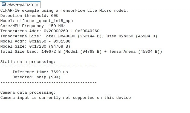
Figure 52: UART output produced during the execution of the TensorFlow Lite Micro CIFAR-10 example.
Several interesting observations can be made from the console output.
First, the application identifies the deployed model as cifarnet_quant_int8_npu, indicating that the example uses a quantised 8-bit neural network specifically prepared for execution using the NPU backend.
Secondly, the application reports both the reserved Tensor Arena size and the amount of memory actually consumed during execution.
| Parameter | Value |
|---|---|
| Model | cifarnet_quant_int8_npu |
| Model Size | 94,768 B |
| Tensor Arena Reserved | 262,144 B |
| Tensor Arena Used | 45,904 B |
| Total Memory Used | 140,672 B |
| Core / NPU Frequency | 150 MHz |
Although a Tensor Arena of 256 KB is reserved, the selected CIFAR-10 model required only approximately 46 KB during execution. This leaves considerable headroom for larger neural networks or more complex inference pipelines while maintaining deterministic memory usage.
Another noteworthy aspect is that the TensorFlow Lite Micro runtime automatically reports the memory consumed by the interpreter, making it straightforward to estimate the RAM requirements of a given model without requiring additional instrumentation.
After the runtime completed its initialisation, the application executed inference using a static test image embedded within the firmware.
The reported classification result was:
This confirms that the complete inference pipeline was operating correctly, including model loading, tensor allocation, execution of the neural network and output post-processing.
Besides demonstrating correct operation, the SDK example also measures the execution time required to perform a complete neural network inference.
For the selected CIFAR-10 model, the reported inference time was:
7699 µs (approximately 7.7 ms)
To evaluate the repeatability of the measurements, the benchmark was executed multiple times following several independent board resets.
The recorded execution times are shown below.
| Run | Inference Time |
|---|---|
| 1 | 7699 µs |
| 2 | 7700 µs |
| 3 | 7699 µs |
| 4 | 7699 µs |
| 5 |
7700 µs |
The average inference time across the five executions was 7699.4 µs, with only 1 µs variation between the minimum and maximum values.
This exceptionally small variation indicates highly repeatable measurements and demonstrates that the benchmark is largely unaffected by run-to-run variability.
Unlike the PowerQuad evaluation presented in the previous chapter, no equivalent CPU-only implementation of the same neural network was supplied within the SDK. Consequently, a direct comparison between Cortex-M33 software inference and NPU-accelerated inference could not be performed during this RoadTest.
Nevertheless, the measured execution time provides a useful reference for future evaluations and confirms that the complete TensorFlow Lite Micro software stack executes successfully on the MCX-N947 platform.
Although the original Test Plan proposed comparing CPU and NPU inference performance, implementing an equivalent CPU-only execution path would require modifying the supplied TensorFlow Lite Micro example or rebuilding the model using a different operator configuration. As this falls outside the scope of evaluating the official SDK examples, the investigation focused instead on analysing the developer workflow, memory requirements and measured inference performance of the NPU-enabled implementation.
From a software engineering perspective, the TinyML support provided within the MCUXpresso SDK leaves a very positive first impression.
Rather than requiring developers to integrate TensorFlow Lite Micro manually, the SDK already includes complete example applications that demonstrate the full deployment workflow, from model initialisation to inference execution and output processing.
Equally important, the integration between TensorFlow Lite Micro and the Neural Processing Unit is largely transparent to the application developer. The firmware itself contains very little hardware-specific code, with TensorFlow Lite Micro managing model execution while dispatching supported operations to the dedicated NEUTRON_GRAPH custom operator executed by the NPU.
This abstraction significantly reduces the complexity typically associated with deploying hardware-accelerated machine learning models on embedded systems.
The runtime information provided through the UART is also particularly useful during development. Memory consumption, Tensor Arena usage, model size and inference timing are all reported automatically, making it straightforward to evaluate whether a model fits within the available hardware resources.
Although this RoadTest did not include training a custom neural network or generating a new TensorFlow Lite model, the supplied examples demonstrate that the software ecosystem is sufficiently mature to allow developers to begin experimenting with TinyML immediately after installing the SDK.
Overall, the Neural Processing Unit should not be viewed as a replacement for the Cortex-M33 processor, but rather as another hardware accelerator within the MCX-N947 platform. In much the same way that the PowerQuad accelerates mathematical computations, the NPU accelerates machine learning inference while allowing the CPU to remain available for the remainder of the embedded application.
The combination of a well-integrated TensorFlow Lite Micro runtime, complete SDK examples and deterministic memory management makes the MCX-N947 an attractive platform for engineers interested in bringing Edge AI capabilities to resource-constrained embedded systems.
After exploring the development environment, SDK structure and hardware acceleration capabilities of the FRDM-MCXN947, the next step was to build a complete embedded application using one of the peripherals already integrated on the board.
For this experiment, I selected the on-board P3T1755 digital temperature sensor, which communicates over the I3C bus, together with the user RGB LED. The objective was to start from the official SDK example and extend it into a more practical demonstration capable of providing both serial output and immediate visual feedback.
Although intentionally simple, this application exercises many of the tasks involved in everyday embedded software development: configuring peripherals, integrating SDK drivers, acquiring sensor data, implementing application logic and controlling hardware outputs.
Beyond demonstrating the functionality of the temperature sensor itself, this exercise also served as an opportunity to evaluate how easily the supplied SDK examples can be adapted into a custom application. From importing the project into MCUXpresso IDE to modifying the firmware and validating the behaviour with real temperature changes, the complete workflow required only a relatively small amount of additional code, allowing development to remain focused on the application rather than low-level hardware configuration.
The FRDM-MCXN947 development board integrates an NXP P3T1755 digital temperature sensor, providing a convenient way to evaluate the I3C peripheral without requiring any additional external hardware. Since the device is already connected on the PCB, temperature measurements can be performed immediately using the software drivers included in the MCUX SDK.
The P3T1755 communicates through the I3C interface and is supported by a dedicated driver within the SDK. The supplied example configures the communication peripheral, assigns the sensor's dynamic address and periodically retrieves the measured temperature, allowing the application to focus on higher-level functionality instead of low-level protocol handling.

Figure 53 : Location of the on-board P3T1755 temperature sensor on the FRDM-MCXN947.
One of the advantages of this arrangement is that the entire sensor demonstration can be implemented using only the resources available on the evaluation board. No additional sensors, wiring or external circuitry are required, making it an ideal starting point for evaluating both the hardware platform and the quality of the software support provided by the SDK.
To establish a known working baseline, I began by importing the official i3c_master_read_sensor_p3t1755 example included with the MCUX SDK. The import process was straightforward and automatically generated a ready-to-build MCUXpresso IDE project with all the required drivers, board support files and middleware already configured.
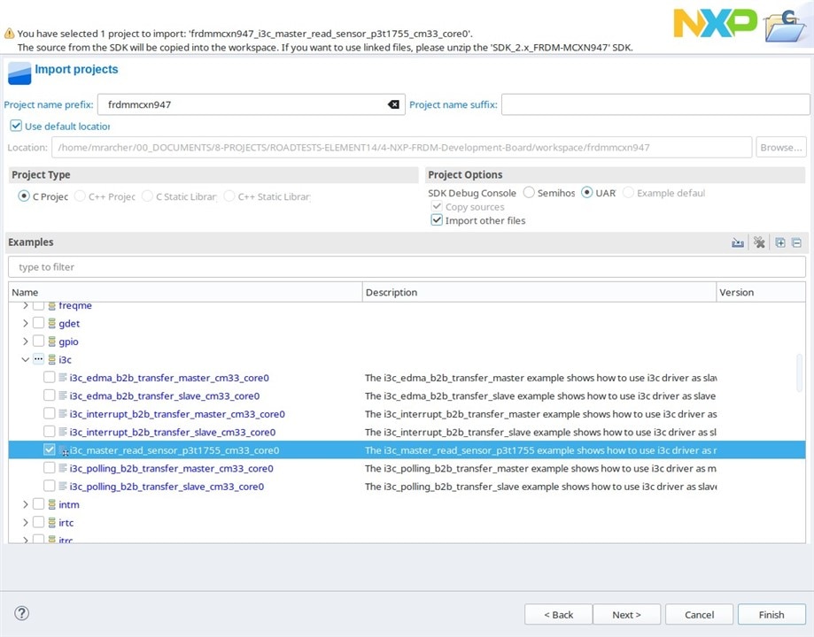
Figure 54 : Importing the i3c_master_read_sensor_p3t1755 SDK example into MCUXpresso IDE.
After the project was imported, the application structure was immediately easy to understand. The main program initializes the board, configures the I3C peripheral, creates the transfer handle and assigns the sensor's dynamic address before initializing the P3T1755 driver.
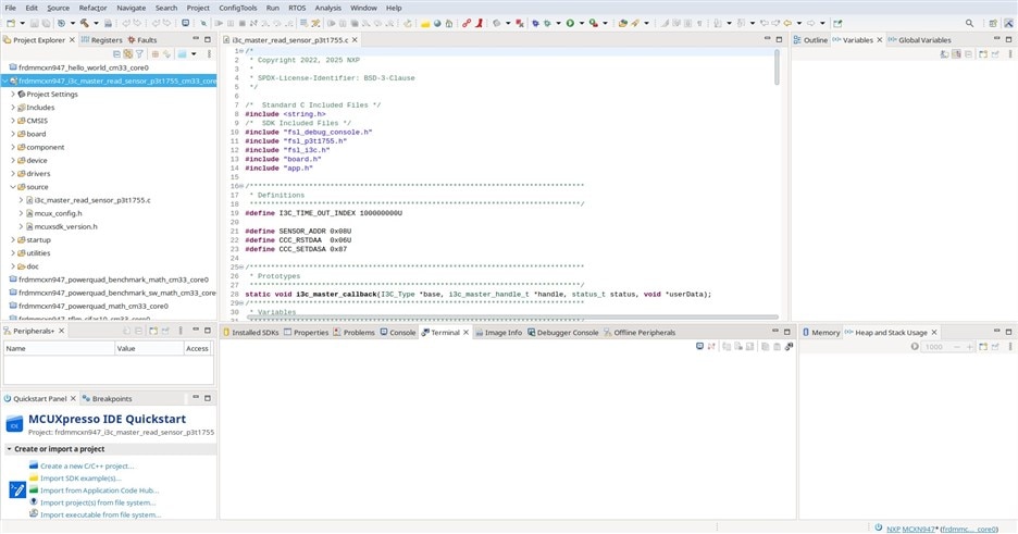
Figure 55 : Main application of the SDK example.
The actual temperature acquisition is abstracted by the P3T1755 driver. The application simply invokes the P3T1755_ReadTemperature() API, while the driver transparently performs the required I3C transactions, reads the sensor registers and converts the raw measurement into degrees Celsius before returning the result.
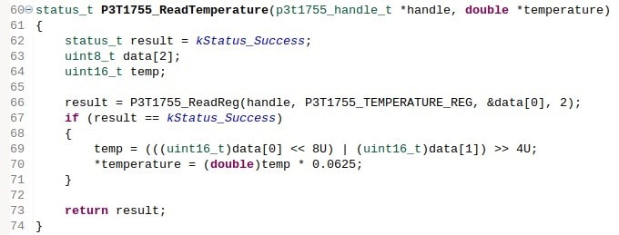
Figure 56 : Temperature acquisition and conversion implemented by the P3T1755 driver.
The project compiled successfully without requiring any modifications, confirming that both the SDK and the board support package were correctly configured.
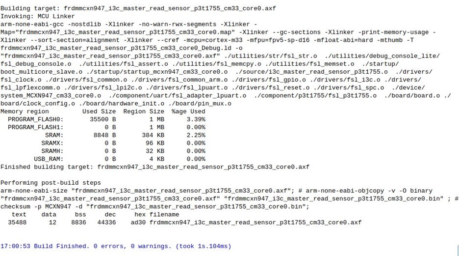
Figure 57 : Successful compilation of the SDK example.
Once programmed into the FRDM-MCXN947, the application periodically reported the measured temperature through the serial console. The reported values were stable and closely matched the ambient room temperature, providing a good reference point before extending the example.
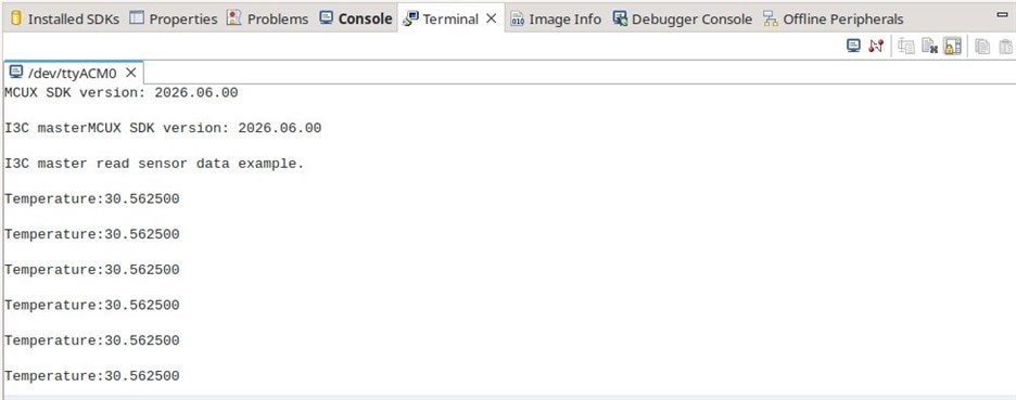
Figure 58 : Serial terminal showing periodic temperature measurements generated by the SDK example.
Starting from a fully functional SDK example significantly reduced the amount of development effort required. Rather than implementing the communication protocol from scratch, I was able to focus entirely on extending the application with additional functionality.
While the original SDK example successfully demonstrated communication with the P3T1755 sensor, its output was limited to periodically printing the measured temperature over the debug UART. To make the demonstration more representative of a real embedded application, I extended the example by using the on-board RGB LED as a visual temperature indicator.
The implementation was intentionally kept simple. Two configurable temperature thresholds divide the measured value into three operating ranges:
| Temperature Range | RGB LED | Interpretation |
|---|---|---|
| T < 18 °C | Blue | Cold |
| 18 °C ≤ T < 28 °C | Green | Normal |
| T ≥ 28 °C | Red | Hot |
The selected thresholds are intentionally arbitrary and are used only to demonstrate the interaction between sensor measurements and user feedback. In a real application these values would typically be configurable according to the target environment.
The first modification consisted of defining the GPIO assignments for each RGB LED channel together with the temperature thresholds. Using symbolic definitions keeps the application easy to modify and allows the thresholds to be adjusted without changing the application logic.

Figure 59 : Temperature thresholds and RGB LED GPIO definitions added to the application.
After each temperature measurement, the firmware first turns all three LED channels off before enabling only the colour corresponding to the current temperature range. This guarantees that only one colour is displayed at any given time.

Figure 60(a) : Main application code implementing the RGB LED temperature indication.

Figure 60(b) : Main application code implementing the RGB LED temperature indication.
The resulting decision logic is intentionally straightforward, making the behaviour easy to understand while clearly illustrating how sensor data can be translated into immediate user feedback.

Figure 61 : Flowchart of the RGB LED decision logic based on the measured temperature.
Despite the additional functionality, the required code changes remained relatively small. The extension consists primarily of GPIO initialization, a simple threshold comparison and updating the RGB LED state, demonstrating how easily the original SDK example can be adapted into a more practical embedded application.
After verifying that the original SDK example was operating correctly, the extended application was tested under different environmental conditions to validate both the temperature measurements and the RGB LED indication.
The first observation was that the measured temperature remained above the upper threshold under normal room conditions, with the application continuously reporting values through the debug UART while illuminating the red LED. This was expected, as the evaluation was performed during the summer and the ambient temperature inside the office was relatively high.
To verify the remaining operating ranges, the on-board P3T1755 sensor was cooled using the airflow from a portable air conditioning unit directed towards the sensor location on the PCB. This provided a simple but effective method for gradually reducing the measured temperature without requiring any specialised laboratory equipment. Rather than simulating temperature changes in software, I wanted to validate the complete sensing chain under real operating conditions.

Figure 62 : Experimental setup used to cool the on-board P3T1755 temperature sensor.

Figure 63 : Detail of the cooling arrangement showing the airflow directed towards the sensor.
As expected, the reported temperature gradually decreased over several measurement cycles, confirming that both the I3C communication and the sensor driver were operating correctly. As the measured temperature crossed the configured thresholds, the firmware automatically switched the RGB LED from red to green, and finally to blue, demonstrating the correct operation of the complete temperature indication logic.
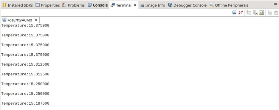
Figure 64 : UART output showing the measured temperature after cooling the sensor.
Finally, the complete RGB indication was verified by exercising all three operating ranges. The firmware correctly selected the appropriate LED colour according to the configured thresholds, providing an immediate visual representation of the measured temperature without requiring a serial terminal.

Figure 65 : RGB LED indication for the three configured temperature ranges: blue (<18 °C), green (18 °C–28 °C) and red (≥28 °C).
Although the experiment itself is intentionally simple, it successfully validates the complete sensing chain: sensor acquisition over I3C, temperature processing in software, application decision logic and visual feedback through the on-board RGB LED. The resulting demonstration is considerably more representative of a real embedded application than the original SDK example, while requiring only a small amount of additional code.
This experiment proved to be an excellent example of the overall development experience offered by the FRDM-MCXN947 platform. Starting from a working SDK example, I was able to understand the software structure, modify the application and validate the new functionality in a relatively short amount of time without having to deal with low-level peripheral implementation.
One of the strongest aspects of the SDK is the clear separation between the application code and the peripheral drivers. The main application simply requests a temperature measurement through the P3T1755 driver, while the underlying I3C communication, device configuration and data conversion remain encapsulated within the SDK. This abstraction allows developers to focus on application behaviour rather than communication details.
The modifications required to transform the original example into a more complete demonstration were intentionally minimal. Besides adding the RGB LED initialization, defining a few configurable thresholds and implementing a simple decision routine, the original software architecture remained unchanged. This demonstrates that the supplied examples provide a solid foundation for developing custom applications rather than serving only as isolated demonstrations.
The physical validation performed using external cooling also provided confidence that the complete sensing chain was operating correctly. The measured temperature responded as expected to environmental changes, the UART output reflected the updated values and the RGB LED changed state automatically according to the configured thresholds. Together, these observations confirmed that sensor acquisition, application logic and hardware control were all functioning as intended.
Although this demonstration is intentionally simple, the same software structure could easily be extended to support more advanced applications such as environmental monitoring, thermal alarms, fan control, data logging, wireless telemetry or cloud-connected IoT devices. The experiment therefore illustrates not only how to use the on-board temperature sensor, but also how quickly an SDK example can evolve into a practical embedded application.
Overall, this exercise reinforced one of the main impressions gathered throughout this RoadTest: the MCUX SDK provides well-structured examples that are easy to understand, straightforward to modify and suitable as the starting point for real product development. From a developer's perspective, the complete application required only a few dozen additional lines of application code beyond the original SDK example, highlighting the usefulness of the provided software framework for rapid prototyping.
Having completed all the experiments presented throughout this RoadTest, it is now possible to evaluate the FRDM-MCXN947 not only from a performance perspective, but also as a complete embedded development platform.
Although the board incorporates advanced hardware features such as the dual Cortex-M33 architecture, the PowerQuad accelerator and the integrated Neural Processing Unit (NPU), the overall user experience depends on much more than raw computational performance. Ease of setup, SDK quality, documentation, software examples and development tools all contribute to determining how quickly an engineer can move from initial evaluation to a functional embedded application.
Throughout this RoadTest, the board was evaluated across multiple aspects, including hardware design, software development workflow, hardware acceleration, machine learning support and practical application development. The following table summarises the main observations gathered during the evaluation.
| Feature | Summary | Rating |
|---|---|---|
| Out-of-the-box Experience | Quick setup with minimal configuration required. | 10/10 |
| Hardware Design | Well-designed PCB with a comprehensive selection of on-board peripherals and expansion interfaces. | 10/10 |
| Documentation | Comprehensive documentation with extensive reference material and SDK integration. | 9.5/10 |
| MCUXpresso IDE | Stable, intuitive and well integrated with the MCU-Link debugger and SDK. | 10/10 |
| MCUX SDK | Mature software framework with a large collection of reusable examples and peripheral drivers. | 10/10 |
| Example Projects | Excellent starting point for understanding peripherals and rapidly developing custom applications. | 10/10 |
| PowerQuad | Excellent DSP acceleration with very little application code required. | 10/10 |
| Neural Processing Unit | Straightforward TinyML deployment with good SDK integration, although the workflow has a steeper learning curve than conventional MCU development. | 9.0/10 |
| Temperature Sensor Demonstration | Demonstrated how easily SDK examples can be transformed into practical embedded applications. | 10/10 |
| Debug Experience | Reliable programming, responsive debugging and seamless MCU-Link integration. | 10/10 |
| Overall Impression | A mature, capable and well-balanced embedded development platform suitable for both evaluation and professional product development. | 9.8/10 |
From an engineering perspective, one of the platform's greatest strengths is the balance between hardware capability and software maturity. Rather than simply providing powerful hardware peripherals, NXP complements the MCX-N947 with a well-structured SDK, comprehensive documentation and an integrated development environment that significantly reduces the effort required to begin experimenting with advanced features.
The practical experiments performed throughout this RoadTest demonstrated that moving from an official SDK example to a fully functional embedded application requires only a relatively small amount of additional code. Features such as the PowerQuad accelerator, the integrated NPU and the on-board P3T1755 temperature sensor illustrate how the platform supports increasingly sophisticated embedded applications while maintaining an accessible development workflow.
Overall, the FRDM-MCXN947 delivers an excellent combination of performance, software support and ease of use. It successfully bridges the gap between evaluation hardware and a professional embedded development platform, making it well suited for rapid prototyping, advanced digital signal processing, Edge AI applications and general-purpose embedded software development.
The following chapters summarise the main strengths of the platform, discuss the few areas where improvements could be made and present my overall conclusions after completing this evaluation.
Throughout this RoadTest, the FRDM-MCXN947 proved to be much more than a development board showcasing individual hardware features. Instead, it presented itself as a complete embedded development platform where the hardware, software tools, SDK and documentation work together to provide a smooth and productive development experience.
While the board includes impressive hardware capabilities such as dual Arm Cortex-M33 cores, the PowerQuad accelerator and the integrated Neural Processing Unit (NPU), what ultimately determines the usability of any development platform is how easily developers can access and exploit those capabilities. In this respect, the MCUXpresso ecosystem plays a fundamental role by providing a mature SDK, a comprehensive collection of example projects and an integrated development environment that significantly reduces the initial learning curve.
The following sections summarise the aspects that stood out most during this evaluation, together with a comparison against other development platforms that I have used in both professional projects and personal development.
Several aspects of the FRDM-MCXN947 left a particularly positive impression during this evaluation.
Although the overall experience was highly positive, a few areas could be further improved to make the platform even more approachable, particularly for developers new to the MCX family.
None of these observations represent significant shortcomings, but addressing them would further improve an already mature development ecosystem.
Throughout my professional work and personal projects I have worked with development platforms from several semiconductor vendors. Each ecosystem targets slightly different application domains, but comparing their overall development experience helps position the FRDM-MCXN947 within today's embedded landscape.
| Platform | Main Strengths | Compared with FRDM-MCXN947 |
|---|---|---|
| Infineon PSoC | Flexible programmable peripherals and strong analogue capabilities. | The FRDM-MCXN947 focuses more heavily on high-performance embedded computation and Edge AI applications. |
| ESP32 | Excellent wireless connectivity and low-cost IoT development. | The MCX platform targets professional embedded applications requiring deterministic real-time performance and hardware acceleration. |
| Arduino | Extremely accessible educational platform with a vast community. | The FRDM-MCXN947 provides significantly greater processing capability and is better suited for professional embedded software development. |
Rather than replacing these platforms, the FRDM-MCXN947 occupies a different position within the embedded ecosystem. Its combination of modern Cortex-M33 cores, dedicated hardware acceleration and a mature software environment makes it particularly attractive for engineers developing computationally demanding embedded applications while retaining the simplicity and determinism expected from a microcontroller platform.
Based on the practical evaluation carried out during this RoadTest, the FRDM-MCXN947 appears particularly well suited for:
Engineers interested in exploring modern Cortex-M architectures, hardware acceleration and embedded machine learning are likely to obtain the greatest benefit from this platform. At the same time, the mature SDK and comprehensive documentation make the learning curve considerably shorter than might be expected for a microcontroller offering this level of functionality.
Overall, the FRDM-MCXN947 successfully combines ease of use with advanced hardware capabilities, making it equally suitable for evaluating the latest MCX architecture, developing proof-of-concept applications and serving as the foundation for professional embedded software development.
The primary objective of this RoadTest was to evaluate the NXP FRDM-MCXN947 not simply as another microcontroller development board, but as a complete embedded development platform capable of supporting modern high-performance applications.
After completing the evaluation, I believe the board successfully achieves that objective. Throughout the RoadTest, the FRDM-MCXN947 consistently demonstrated an excellent balance between hardware capabilities, software maturity and overall ease of development. From the initial out-of-the-box experience to implementing custom applications using the on-board peripherals, the development workflow remained intuitive, reliable and well supported by the MCUXpresso ecosystem.
One of the platform's greatest strengths is that its advanced hardware features are backed by an equally mature software environment. Powerful capabilities such as the dual Cortex-M33 architecture, the PowerQuad accelerator and the integrated Neural Processing Unit would be of limited value without a comprehensive SDK, high-quality documentation and practical example projects. Fortunately, NXP delivers all three, making these advanced features significantly more accessible than might initially be expected.
The practical experiments carried out during this RoadTest confirmed that moving from official SDK examples to fully functional embedded applications requires relatively little additional effort. Whether exploring digital signal processing, embedded machine learning or general peripheral development, the platform provides a solid foundation that allows developers to focus on application design rather than low-level hardware configuration.
No development platform is entirely without compromise. The richness of the SDK and documentation can initially appear overwhelming, particularly for developers unfamiliar with the MCX ecosystem. However, this is largely a consequence of the platform's breadth of capabilities rather than a weakness of the ecosystem itself. Once the overall software architecture becomes familiar, development progresses quickly and efficiently.
Based on the experience gained throughout this RoadTest, I would confidently recommend the FRDM-MCXN947 to embedded software engineers, students and researchers interested in modern Cortex-M microcontrollers, digital signal processing, Edge AI and rapid embedded prototyping. It is equally suitable as a learning platform for exploring the MCX family and as a professional evaluation board for developing real embedded applications.
Overall, the FRDM-MCXN947 proved to be a highly capable development platform and consistently delivered a smooth development experience throughout this RoadTest. Its combination of excellent hardware, a mature software ecosystem and a productive development workflow makes it well suited to a wide range of embedded applications.
Final Rating: 9.8 / 10
The FRDM-MCXN947 is one of the most complete and well-balanced Cortex-M development platforms that I have had the opportunity to evaluate, and I would have no hesitation in using it again for future embedded development projects.
The following hardware and software environment was used throughout this RoadTest. Unless otherwise stated, all experiments, benchmarks and demonstrations were performed using this configuration.
| Item | Configuration |
|---|---|
| Development Board | NXP FRDM-MCXN947 |
| MCU | MCX-N947 Dual Arm Cortex-M33 |
| Host PC | AMD Ryzen 7 8700G, 32 GB RAM |
| Operating System | Ubuntu 24.04 LTS (64-bit) |
| Development Environment | MCUXpresso IDE |
| MCUXpresso IDE Version | MCUXpresso IDE v25.6.0 (Build 136, 2025-06-27) |
| MCUX SDK Version | MCUX SDK 2026.06.00 |
| Compiler | arm-none-eabi-gcc (MCUXpresso Toolchain) |
| Debug Probe | On-board MCU-Link |
| Debug Interface | SWD |
| Build Configuration | Debug |
Unless explicitly stated otherwise, all software examples were based on the official MCUX SDK projects supplied by NXP and modified only where necessary to perform the experiments described throughout this RoadTest.
The following official documentation and development resources were used during the preparation of this RoadTest.
Additional information was obtained from the official NXP Developer Community and the MCUXpresso online documentation whenever clarification of specific SDK features or development workflows was required.
I would like to sincerely thank NXP and the element14 RoadTest Program for providing the FRDM-MCXN947 development board used throughout this evaluation.
Participating in this RoadTest provided an excellent opportunity to explore the capabilities of the new MCX platform in depth, from basic peripheral development to hardware-accelerated DSP and TinyML applications. I hope that the practical experiments, observations and conclusions presented in this review will help other embedded developers evaluate the platform and reduce the learning curve when getting started with the MCX family.
Finally, I would also like to thank the engineers and developers who contribute to the MCUX SDK, documentation and technical support resources, which played an important role in the successful completion of this RoadTest.


