RoadTest: NXP LPC8N04 Dev Board with Integrated NFC
Author: fyaocn
Creation date:
Evaluation Type: Development Boards & Tools
Did you receive all parts the manufacturer stated would be included in the package?: True
What other parts do you consider comparable to this product?: NA. Power harvesting SoC chip is only available on LPC8N04.
What were the biggest problems encountered?: SDK is not available from official website. It is directly supported by Keil. Only user manual and no SDK API is opened for now. It is reasonable for one new products. hopefully, it would be improved later.
Detailed Review:
1. Brief Introduction
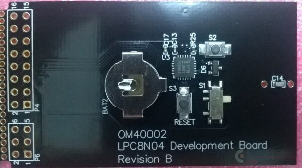
The LPC8N04 Development Board board includes LPC8N04 Arm Cortex-M0+ MCU running at up to 8MHz , Integrated NFC antenna , Dual coin cell battery holders for , On-board CMSIS-DAP (debug probe) with VCOM port,1x User button , 1x Reset button, Surface mounted speaker with amplifier and 5x7 LED array for user applications
LPC8N04 features ISO/IEC 14443 A 1-3 compatible and MIFARE (Ultralight) compatible,in same bandwidth of 13.56MHz.
- Nother feature is that user can be access the Flash address that shared with 4K bit of the chip. Fom APB side 0x4005 8100 to 0x4005 82FC,from RFside 0x04 to 0x83。
- Internal 50 pF capacitor , compatible for standard NFC antenna.
- RFID clock on 6.78MHz from RF signal which is independent of master clock of chip LPC8N04.
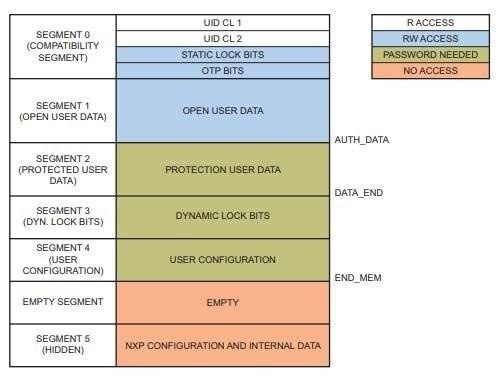
Here is the memory map,
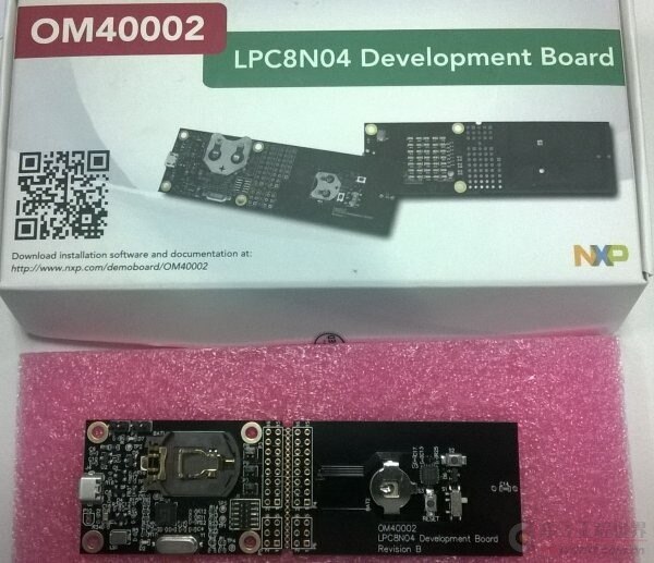
2. Unboxing
2.1 the complete development kit
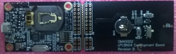
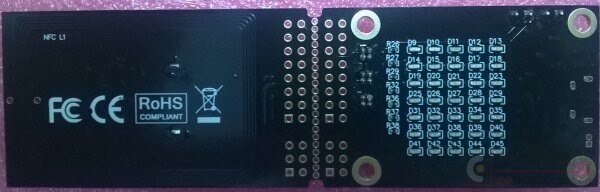
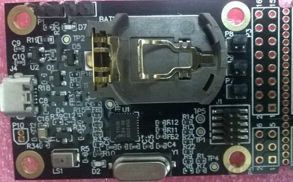
Close look on both sides of the board,
The board can be detachable with multiple power source, USB, battery from master part or battery from detached daughter board, or wireless power delivery from NFC mobille.
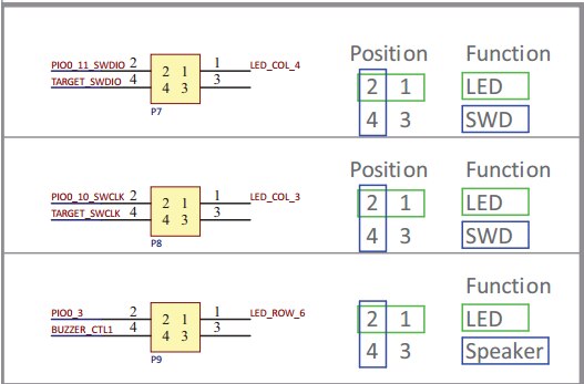
2.2 SWD/Speaker/LED selection jumpers shall be selected before running
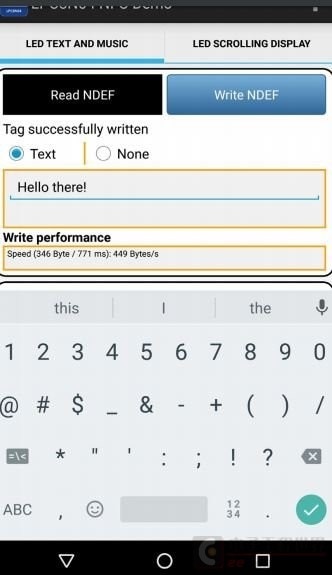
search for NXP LPC8N04 NFC Demo in google play,
enable the NFC board with mobile approximated with APP running in Read/ Write
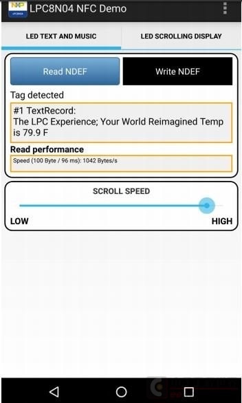
press write then the text shall be displayed in the LED array
2.3 Video,of Plugin and power on, one column of LED flash in turns before NFC is wake up.
3 The NFC protocol
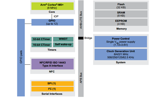
3.1 The MCU block diagram shows the configuration of the LPC8N04
3.2 The NFC runs in one of the three mode,
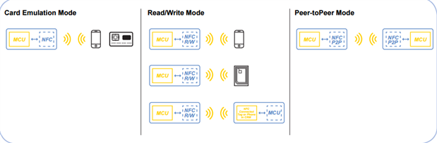
In the factory demo program , Read/Write mode is used.
3.3 The best application for LPC8N04 is the energy harvest mode as follows,
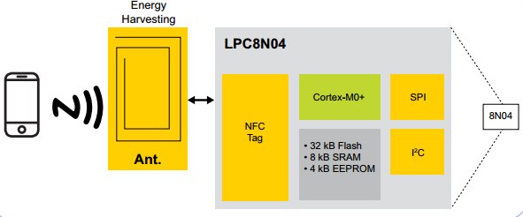
In this mode, the LPC8N04 can retrieve power from mobile with data acquisition and power extraction.
This mode is the main part of this roadtest, I would use this mode to drive e-paper panel or LEDs without classic power supply like battery or USB.
System clock SFRO is 8MHz and can be reduced to 62.5kHz. Default 500kHz after reset in order or power-saving mode.
There are two power source for LPC8N04, internal and outer source selected by PSWBAT pin, as follows
- When outer source VBAT is greater than 1.72V, VBAT and VNFC is active at same time, VBAT is first choice;
- When VBAT is less than 1.72V,and VNFC is greater than 1.72V,VNFC is active;
- VNFC and VBAT can switch over quickly, if another source lost power. if larger load is used , one 100nF shall be paralleled in order for voltage stable.
3.4 Near Field Communication (NFC) is a technology that enables smartphones, and many other devices, to establish radio communication by bringing them into close proximity. Typically NFC has a range of 10 cm (3.9 in) or less. The RFID/NFC interface allows communication using 13.56 MHz proximity signaling. It is based on the MIFARE Ultralight EV1 PICC. The RFID interface works internally at 6.78 MHz.
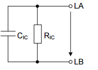
3.5 Equivalent circuit of the NTAG IC
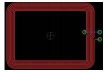
with coil design such as,
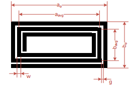

in this development board, class 6 coil is used as,
4. Development Tools
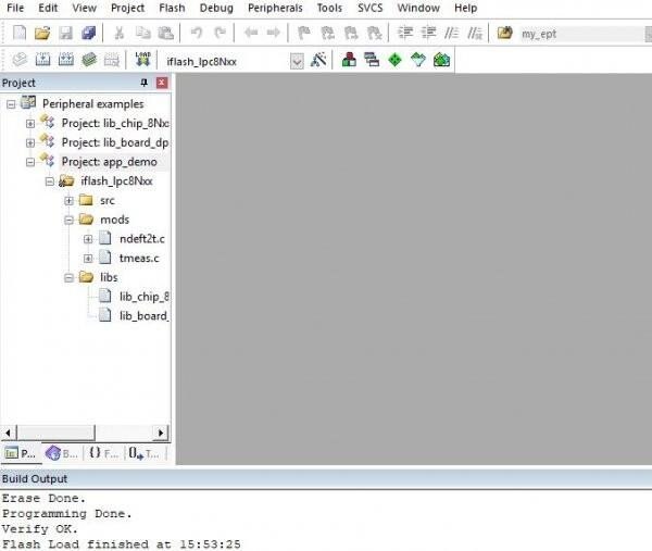
4.1 kEIL can be used with demo file as follows
4.2 Another tools is FlashMagic, it can be installed with hex file flash
5. Next Roadtest shall be one project display text with energy harvest feature for LCD panel in SPI
To be continue for this simple project


