RoadTest: Synchronous Step-Down Converter Evaluation Module
Author: jdlui
Creation date:
Evaluation Type: Evaluation Boards
Did you receive all parts the manufacturer stated would be included in the package?: True
What other parts do you consider comparable to this product?: n/a
What were the biggest problems encountered?: Modifying output voltage is near impossible without a good soldering iron and skill. finding hardware to test with it (I recently moved out of country and have few lab supplies)
Detailed Review:
This is my first time doing a review on something that isn't a microcontroller! And in many ways I thought this would be easier, but it turns out that there are many aspects of this I truly didn't understand.
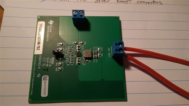
The TI TPS56C215EVM-762 12-A, SWIFT™ Regulator Evaluation Module is in short just an Eval module for a new TI buck converter (step-down converter). On this eval module is the new TI TPS56C215 chip. It's a tiny little surface mount DC/DC converter that is able to provide output currents as high as 14A. It operates on similar principles of other buck converters: it is a switched mode power supply, meaning that it rapidly switches on and off to moderate the current and voltage output. This means that it is much more power efficient than linear voltage regulators, which are dissipating excess energy as heat energy. However the rapid switching of the supply may not be suitable to all applications. Sometimes a "wasteful" linear voltage regulator is still preferred when a very low noise supply is desired.
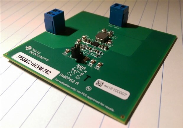
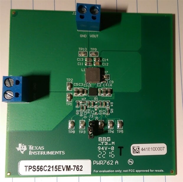
Pretty board.
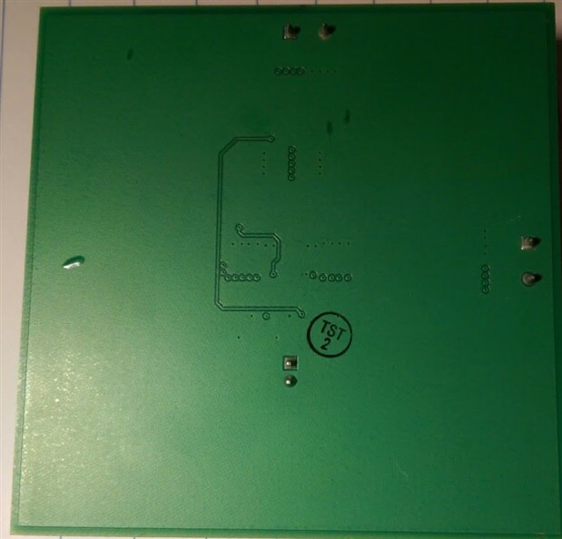
The Back
The Eval module as delivered is configured for a 4.5-17V input and to output 1.2V with current ranging from 0-12A. The datasheet states maximum efficiencies of 82.2% can be achieved with a 5V supply and a 5.7A output.
First impressions: It arrives in a sleek, well-padded foam package. The board looks good and clean. There is pretty much no documentation, but most of us have regular internet access today anyways.
This Eval module does allow testing at other voltage levels, by changing the output voltage setpoint. As a casual electronics user, I find their explanation in the datasheet somewhat lacking. It sounds like I need desolder a little SMT resistor at the R7 position, or at least solder two leads against it, but this is pretty messy work just to test the converter at different voltages.
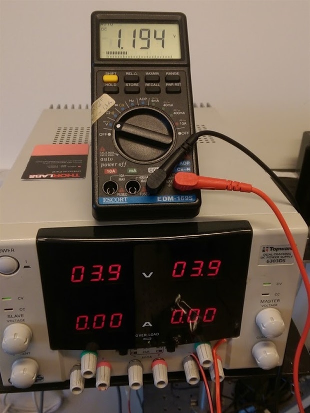
Datasheet states a input voltage range from 4.5 to 17V. I noticed that an output voltage of 1.194V starts to appear when a voltage of 4.3V is supplied. However, if you slowly decrease the voltage, you can get as low as 3.9V before it switches off. Switch on at 4.3V, drops off at 3.9V.
The datasheet claims Line Regulation of +/- 0.05% on a 6A load and Load regulation of -0.02% and +0.6% for all loads 0A-12A on a 12V supply. I did a very basic test with no load and varying voltages and found the following variations. I notice that the actual voltage output is slightly less than 1.2V, but perhaps this is reasonably close. In trying a variety of input voltages, the output voltage never varies more than 0.17% from the Voltage out in the 12V supply scenario.
Vi | Vo, no load | Deviation from Setpoint | Deviation from 12V supply |
4.1 | 1.194 | 0.50% | 0.00% |
5 | 1.194 | 0.50% | 0.00% |
6 | 1.194 | 0.50% | 0.00% |
8 | 1.194 | 0.50% | 0.00% |
10 | 1.194 | 0.50% | 0.00% |
12 | 1.194 | 0.50% | 0.00% |
15 | 1.193 | 0.58% | 0.08% |
17 | 1.192 | 0.67% | 0.17% |
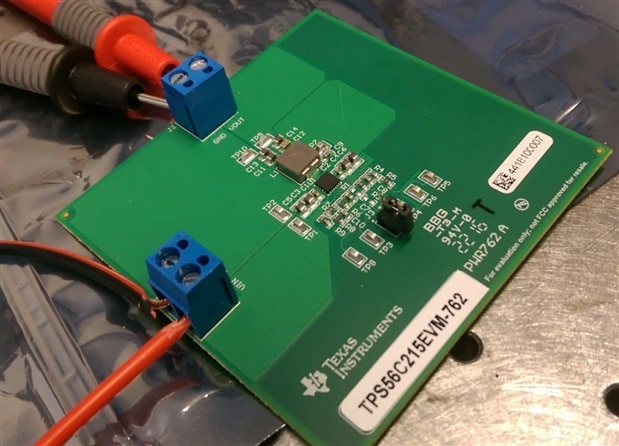
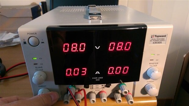
My next test was the power efficiency of the output. I really underestimated this portion of the review, since I hadn't worked with high current loads much before. I didn't have any big rugged testing equipment or anything I could repurpose as a high current load, so I just used the high wattage resistors in my lab. I've recently moved to Italy for a few months and I'm really having some trouble finding precision electronics in my lab. I could only find a Topward 6303DS power supply with 3 digits of precision on my voltage and current output. So be it.
I realized soon on in this review that I lacked much of electronics that I'd need to really put this board through its paces. The main test I was able to do was verify the output efficiencies at a couple of current values. Overall my setup was extremely rudimentary, and definitely not optimal. I found the heaviest gauge wires I could to wire up my input and output, and used the only high wattage resistors I could find in my lab. I notice Gough Lui had a nifty adjustable load device, I guess this is precisely the time to have one of these!
I was pretty limited in my high wattage resistor hardware so I simply combined resistors in series and in parallel to get a variety of resistances. I was careful to check that I wasn't exceeding wattage ratings. I was concerned about the current values I would experience and didn't want to damage any lab electronics or breadboards. So I ended up making the following abominations.
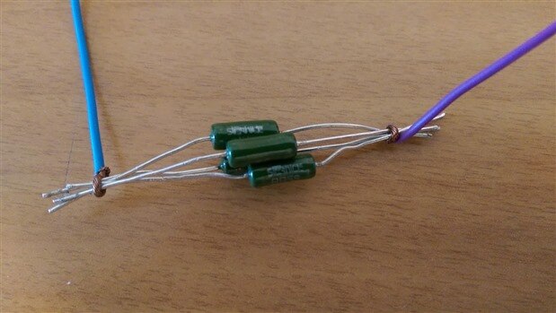
It's good I'm not pursuing an Elec Eng degree. Someone would come shut me down. This is 4 3R resistors in parallel. That's an equivalent resistance of 0.75R. At 1.2V this will draw 1.6A, or 1.92W. The resistors are each rated for 3W so we have no issues here.
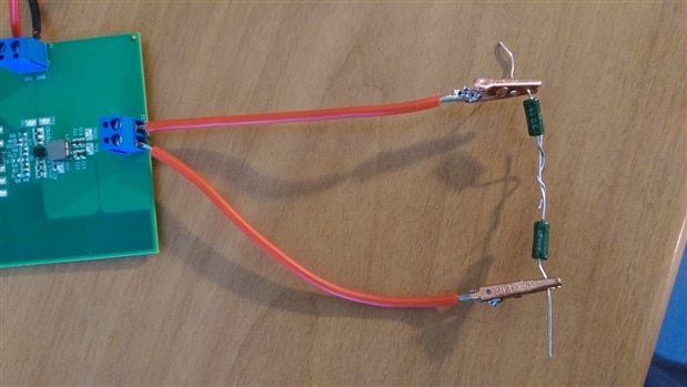
I tried to clip as close to the resistors as possible
Because I had some early issues with low wattage resistors heating up and increasing in resistance, I chose to drive the eval module through a slave supply so that I could de-couple my voltage setting from the current setting. So I would set my voltage on one side while the current output was 0. Then I would quickly allow some current into my converter, note the current output, and then switch it off again. Decreased the resistor heating by a degree, and should increase my accuracy.
Took several readings, and got the following result! What you see below is that the overall efficiency is higher at lower voltages. Converter efficiency is generally lower for a higher voltage input.
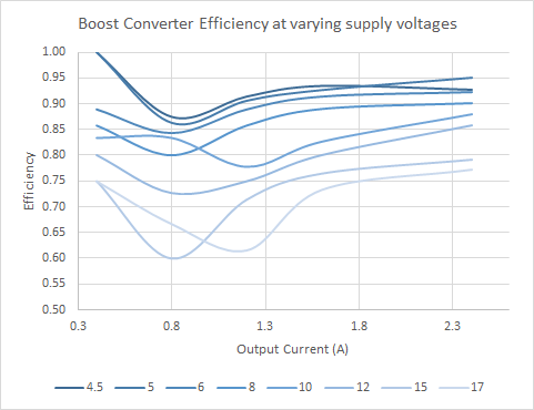
This efficiency trend is consistent with what Gough Lui encountered and with what is listed in the datasheet. I had initially set out this evaluation with the intent to verify efficiencies at lower current values. However I clearly was not thinking about using my multimeter to measure current, and ended up limiting my measurement accuracies by only measuring through the power supply's 3 digit precision. A lesson for the future I guess.
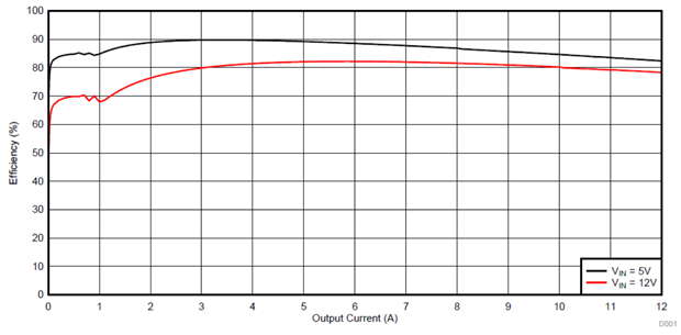
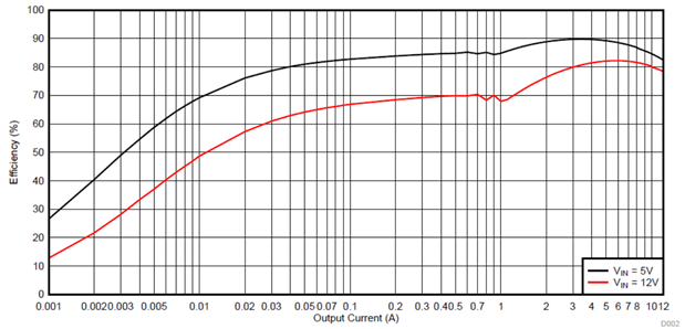
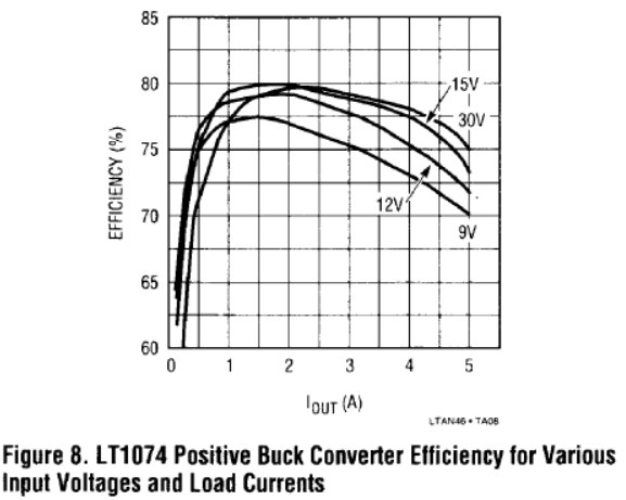
I was reading through an application note from Linear Technologies on buck and boost converters and saw the following efficiency trend. I was confused why their efficiencies increase with increasing voltage, while efficiencies in the TI chip go down with increasing voltage. This seems very odd to me, but I'm likely missing some fundamental difference between the two. Note that this is an application note from 1991; and the overall performance of the TI chip is much higher overall. Note the steep drop in efficiency that occurs around 1A for the LT1074. In contrast, the TI chip performs quite gracefully until 0.1A, when the efficiency starts to sharply drop. I was curious why the TI chip's efficiency is very odd around 1A, but did not find anything to explain this oddity.
In summary this seems like a sturdy dandy of an eval board if you're considering incorporating one of these chips into your products. The chip is incredibly small and quite power efficient, and yet can deliver a punch in terms of current. However from the eval board point of view, it is not built to allow easy modification of the output voltage, unless you want to do some tricky soldering onto the edges of a SMD resistor. Not fun!
My recommendation would be that this Eval board should have a more accessible R7 and R9 for modification of the output voltage.


Top Comments
Thanks for the review.
Jordan,
It's late now and I saw your review. Without any interruptions, which is common at the office, I read your review. I enjoyed it. I'm passing it on to my contact at Texas Instruments. I think they…
The switching node waveform goes between the supply voltage and a fraction below ground. It may overshoot to a volt or two below ground before the bottom MOSFET hauls it back to within a few hundreds of…