RoadTest: AVNET MicroZed™ Evaluation Kit
Author: b_smith
Creation date:
Evaluation Type: Independent Products
Did you receive all parts the manufacturer stated would be included in the package?: True
What other parts do you consider comparable to this product?:
What were the biggest problems encountered?: Connecting to Terminal via UART whilst the Microzed was plugged into carrier card
Detailed Review:
Contents:
Introduction
Unpacking
MicroZed 7010
Design Process
Setup
Tutorials:
Hello World
Quadrature Decoder
Conclusion
Introduction
Thanks to Randall and the element14 team for selecting me for this review. I am a student from Melbourne Australia, studying Bachelor of Electrical Engineering. Various units in my course have given me experience with FPGAs. The reason I applied for this review is because my final year project involves building a 4 band parametric audio equalizer with a Xilinx Zynq 7010 SoC, so I have had experience using this chip since the start of the year. The main part of this review consists of a detailed step by step tutorial on how to implement quadrature decoder logic for an incremental encoder. It is intended for people who have not used Vivado software and want to get started with a practical project. I am still learning, so keep in mind that my design may not be the best solution.
Unpacking
The MicroZed arrived in Australia about a week after I was notified that I had been selected. It was very well packed and included a micro SD card, USB cable and Digilent JTAG cable.


MicroZed 7010
The AVNET MicroZed 7010 contains a Xilinx ZYNQ 7010 SoC which integrates an ARM based processor (PS) with programmable FPGA fabric (PL). Included on the board is a JTAG header, micro USB for power and UART communication, Ethernet , SD card socket and USB host 2.0. User I/O connectivity is limited to a single PMOD port which is interfaced to the PS. The rest of the I/O is accessed via two 100 pin micro headers located under the board.


An expansion board is required to access the micro header pins. Initially I planned on building my own expansion board, but due to time constraints I ended up purchasing an MBCC-BKO Breakout Carrier Card. The Breakout Carrier Card contains a micro USB which supplies only power (whilst plugged into the carrier card, the MicroZed’s micro USB power connection becomes disabled). The I/O pins are accessible via two standard 60 pin connectors. The centre area of the carrier card contains prototyping area, 5V, 3.3V and ground connections.


Design Process
For those who have not used a Zynq SoC FPGA before, the design process involves using the program Vivado to create a block design which can consist of:
Zynq processor (built in dual core ARM cortex A9 processor)
| Microblaze processor (implemented in FPGA fabric)
|
Xilinx IP blocks (implemented in FPGA fabric)
| Create your own IP blocks (implemented in FPGA fabric)
|
The design is synthesised, routed and the hardware file is exported to the Software Development Kit (SDK). The user can then write software to run on the processor and interact with the FPGA hardware.

Communication between the software and hardware is achieved via the AXI interface. The software can read and write to a set of registers within an AXI IP block.

Setup
I already have Vivado 2018.3 installed, the installation process will not be covered in this review. Information can be found on the Xilinx website:
https://www.xilinx.com/support/download/index.html/content/xilinx/en/downloadNav/vivado-design-tools.html
In order to start using the MicroZed, two things are needed:
Board definition files
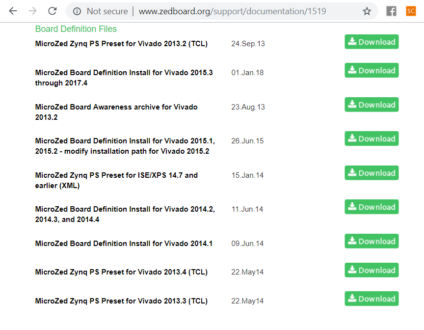
Download and install board definition files from http://www.zedboard.org/support/documentation/1519
These files are used for the configuration of Vivado with the MicroZed settings. Extract the contents of the zip file into C:\Xilinx\Vivado\2018.3\data\boards\board_files
UART driver
Download and install the Silicon Labs CP2104 USB-to-UART driver
https://www.silabs.com/products/development-tools/software/usb-to-uart-bridge-vcp-drivers
This driver is required for communication from the terminal to the Microzed.
Connect micro-usb and JTAG:

Hello World:
In this project Vivado is used to create a basic design that includes only the Zynq processor to run a hello world program which will be viewed on the terminal.
The purpose of this project is a quick way to verify that the tools and the Microzed are working correctly. The carrier card is not used for this project.
Step 1: Open Vivado and create a new project.
Step 2: Enter project name (ensure there are no spaces in the name or file path (including folder names)).
Step 3: Click next.
Step 4: Select “RTL Project”, Click next until you arrive at Default Part dialog.
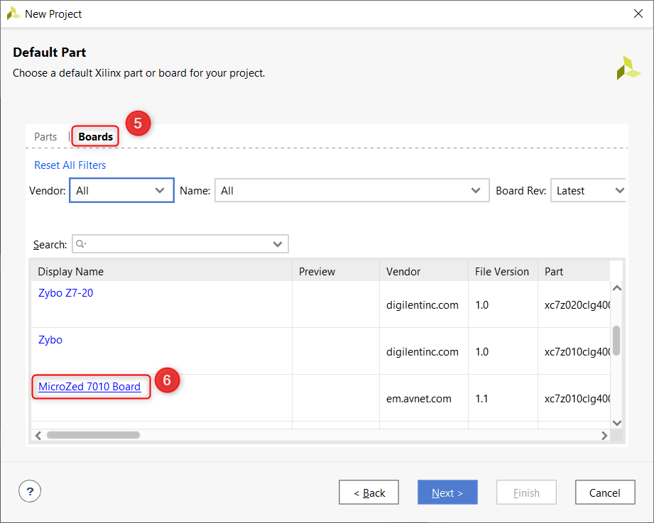
Step 5: Select “Boards”
Step 6: Select MicroZed 7010 Board, Select next, finish.
Step 7: Create Block Design
Step 8: Enter design name, click OK.
Step 9: Click “Add IP”.
Step 10: Search for Zynq Processing System, double click to add IP block to the design.
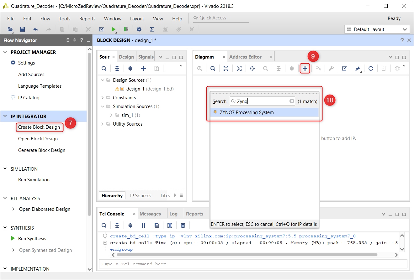
Step 11: Click ‘Run Block Automation’, this will configure the Zynq processor for the Microzed.
Step 12: Double click on the Zynq IP block.
Step 13: Navigate to MIO Configuration, ensure that UART 1 interface is checked. Click OK.

Step 14: In the sources tab, right click on your design and select “Create HDL Wrapper”. Click OK.
Step 15: Once the wrapper is complete, Click “ Generate Bitstream. This will perform all steps from Synthesis to Implementation to generating the Bitstream.
Depending on your computer and the complexity of your design, this step can take some time. For me it takes around 2 minutes. Once complete, a dialog window will appear, click Cancel.
Step 16: Navigate to File > Export > Export_Hardware.
Ensure that “Include Bitstream” is checked and click OK.
That’s it for the hardware, the next step is to navigate to File > Launch SDK.
SDK
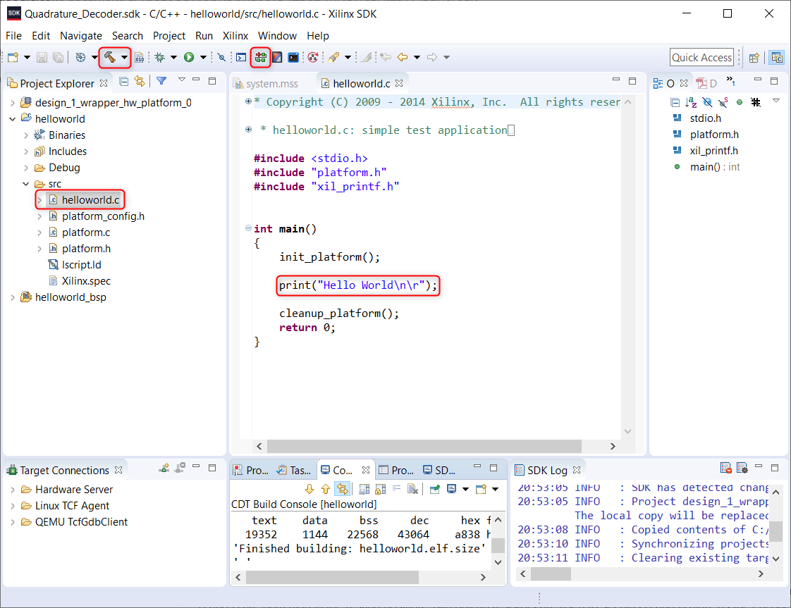
Click File > New > Application Project.
Create a C project, click Next, select hello world, click Finish.
Navigate to the C project folder > src > helloworld.c
Type something in the print statement, click on the hammer to build the project, click on the program icon to program the FPGA,
Click Debug > Debug As > 1 Launch on Hardware
Click Window > Show View > Other > Terminal, OK.
Click Settings in the new terminal window, select Serial as the connection type and 115200 as the Baud Rate.
Press Resume, if everything worked correctly, you will see Hello World in the terminal.

Quadrature Decoder
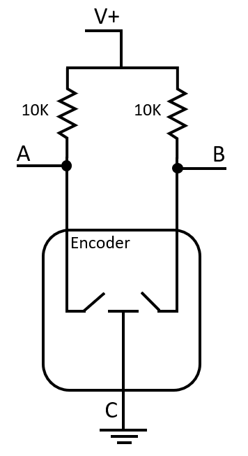
Incremental quadrature encoders generally have three terminals, A, B and C (ground). As the shaft is turned, a sequence of offset square waves appear at the A and B terminals which can be used to determine direction of rotation. A and B are both high in the resting position. Two pull up resistors are used to set pins A and B high, as the encoder is turned, pins A and B are sequentially grounded to create the offset square wave output. This encoder makes four transitions over each indent, depending on which direction it is turned, the sequence will be different.

The design is implemented using the PL fabric and the PS to determine when an incremental encoder has been turned and in which direction. The debounce circuit is based off an existing design. I have added a state machine to detect direction and set a new measurement flag, and some logic to communicate with the processor.
Two registers, a direction register and a flag register are used to allow the PL and PS to communicate via the AXI bus.
The code running on the processor will be continuously polling the flag, when the flag is set high, the code reads in the value from the direction register. Some code has been added to the AXI VHDL to reset the flag register whilst the direction register is read.
Inputs A and B are fed into two flip flops which are used for edge detection in the debouncing circuit. As the input is bouncing, SCLR will be clearing the counter. Once the input stabilizes, the counter will reach the debounce time and set the final flip flops with the stable value. My diagram might not follow exactly what I’ve written in VHDL, but it illustrates the general idea.
The state machine is designed to set the left turn or right turn value high when it detects the correct sequence.
For example, when turning the encoder left, the sequence of AB will be 11, 10, 00, 01, 11. When the transition from 01 to 11 is detected, Left_Turn and Set_Flag are set high.
The states are also designed to account for any unexpected transition that may arise due to errors and to prevent it becoming locked in any state. For example, if the state machine detects 11, 00, 11, it will return to State_On without signalling any increment.
Follow the hello world instructions up to the end of step 13.
Step 14: Navigate to PS-PL Configuration, ensure that M AXI GP0 interface is checked. Click OK.
Step 15 navigate to Tools > Create and Package New IP, Next, Create AXI4 Peripheral, use all default values, Finish.
Step 16: Click IP Catalog.
Step 17: Right click your IP, click Edit in IP Packager.
Once the new window is open, navigate to the source tab, there are two files that need editing:
1: The outer VHDL module
2: The inner VHDL module
Outer VHDL Module
Add the green code and delete the red code:
library ieee;
use ieee.std_logic_1164.all;
use ieee.numeric_std.all;
entity Quad_Decoder_v1_0 is
generic (
-- Users to add parameters here
-- User parameters ends
-- Do not modify the parameters beyond this line
-- Parameters of Axi Slave Bus Interface S00_AXI
C_S00_AXI_DATA_WIDTH : integer := 32;
C_S00_AXI_ADDR_WIDTH : integer := 4
);
port (
-- Users to add ports here
a: in std_logic;
b: in std_logic;
-- User ports ends
-- Do not modify the ports beyond this line
-- Ports of Axi Slave Bus Interface S00_AXI
s00_axi_aclk : in std_logic;
s00_axi_aresetn : in std_logic;
s00_axi_awaddr : in std_logic_vector(C_S00_AXI_ADDR_WIDTH-1 downto 0);
s00_axi_awprot : in std_logic_vector(2 downto 0);
s00_axi_awvalid : in std_logic;
s00_axi_awready : out std_logic;
s00_axi_wdata : in std_logic_vector(C_S00_AXI_DATA_WIDTH-1 downto 0);
s00_axi_wstrb : in std_logic_vector((C_S00_AXI_DATA_WIDTH/8)-1 downto 0);
s00_axi_wvalid : in std_logic;
s00_axi_wready : out std_logic;
s00_axi_bresp : out std_logic_vector(1 downto 0);
s00_axi_bvalid : out std_logic;
s00_axi_bready : in std_logic;
s00_axi_araddr : in std_logic_vector(C_S00_AXI_ADDR_WIDTH-1 downto 0);
s00_axi_arprot : in std_logic_vector(2 downto 0);
s00_axi_arvalid : in std_logic;
s00_axi_arready : out std_logic;
s00_axi_rdata : out std_logic_vector(C_S00_AXI_DATA_WIDTH-1 downto 0);
s00_axi_rresp : out std_logic_vector(1 downto 0);
s00_axi_rvalid : out std_logic;
s00_axi_rready : in std_logic
);
end Quad_Decoder_v1_0;
architecture arch_imp of Quad_Decoder_v1_0 is
-- component declaration
component Quad_Decoder_v1_0_S00_AXI is
generic (
C_S_AXI_DATA_WIDTH : integer := 32;
C_S_AXI_ADDR_WIDTH : integer := 4
);
port (
S_AXI_ACLK : in std_logic;
S_AXI_ARESETN : in std_logic;
S_AXI_AWADDR : in std_logic_vector(C_S_AXI_ADDR_WIDTH-1 downto 0);
S_AXI_AWPROT : in std_logic_vector(2 downto 0);
S_AXI_AWVALID : in std_logic;
S_AXI_AWREADY : out std_logic;
S_AXI_WDATA : in std_logic_vector(C_S_AXI_DATA_WIDTH-1 downto 0);
S_AXI_WSTRB : in std_logic_vector((C_S_AXI_DATA_WIDTH/8)-1 downto 0);
S_AXI_WVALID : in std_logic;
S_AXI_WREADY : out std_logic;
S_AXI_BRESP : out std_logic_vector(1 downto 0);
S_AXI_BVALID : out std_logic;
S_AXI_BREADY : in std_logic;
S_AXI_ARADDR : in std_logic_vector(C_S_AXI_ADDR_WIDTH-1 downto 0);
S_AXI_ARPROT : in std_logic_vector(2 downto 0);
S_AXI_ARVALID : in std_logic;
S_AXI_ARREADY : out std_logic;
S_AXI_RDATA : out std_logic_vector(C_S_AXI_DATA_WIDTH-1 downto 0);
S_AXI_RRESP : out std_logic_vector(1 downto 0);
S_AXI_RVALID : out std_logic;
S_AXI_RREADY : in std_logic
);
end component Quad_Decoder_v1_0_S00_AXI;
begin
-- Instantiation of Axi Bus Interface S00_AXI
Quad_Decoder_v1_0_S00_AXI_inst : entity work.Quad_Decoder_v1_0_S00_AXI
generic map (
C_S_AXI_DATA_WIDTH => C_S00_AXI_DATA_WIDTH,
C_S_AXI_ADDR_WIDTH => C_S00_AXI_ADDR_WIDTH
)
port map (
a => a,
b => b,
S_AXI_ACLK => s00_axi_aclk,
S_AXI_ARESETN => s00_axi_aresetn,
S_AXI_AWADDR => s00_axi_awaddr,
S_AXI_AWPROT => s00_axi_awprot,
S_AXI_AWVALID => s00_axi_awvalid,
S_AXI_AWREADY => s00_axi_awready,
S_AXI_WDATA => s00_axi_wdata,
S_AXI_WSTRB => s00_axi_wstrb,
S_AXI_WVALID => s00_axi_wvalid,
S_AXI_WREADY => s00_axi_wready,
S_AXI_BRESP => s00_axi_bresp,
S_AXI_BVALID => s00_axi_bvalid,
S_AXI_BREADY => s00_axi_bready,
S_AXI_ARADDR => s00_axi_araddr,
S_AXI_ARPROT => s00_axi_arprot,
S_AXI_ARVALID => s00_axi_arvalid,
S_AXI_ARREADY => s00_axi_arready,
S_AXI_RDATA => s00_axi_rdata,
S_AXI_RRESP => s00_axi_rresp,
S_AXI_RVALID => s00_axi_rvalid,
S_AXI_RREADY => s00_axi_rready
);
-- Add user logic here
-- User logic ends
end arch_imp;
Inner VHDL Module
Add the green code and delete the red code:
(some code has been removed for simplicity)
library ieee;
use ieee.std_logic_1164.all;
use ieee.numeric_std.all;
USE ieee.std_logic_unsigned.all;
entity Quad_Decoder_v1_0_S00_AXI is
generic (
-- Users to add parameters here
counter_size : integer := 19;
-- User parameters ends
-- Do not modify the parameters beyond this line
-- Width of S_AXI data bus
C_S_AXI_DATA_WIDTH : integer := 32;
-- Width of S_AXI address bus
C_S_AXI_ADDR_WIDTH : integer := 4
);
port (
-- Users to add ports here
a: in std_logic; -- Encoder A input
b: in std_logic; -- Encoder B input
-- User ports ends
-- Do not modify the ports beyond this line
);
end Quad_Decoder_v1_0_S00_AXI;
architecture arch_imp of Quad_Decoder_v1_0_S00_AXI is
------------------------------------------------
---- Signals for user logic register space example
--------------------------------------------------
---- Number of Slave Registers 4
signal slv_reg0 :std_logic_vector(C_S_AXI_DATA_WIDTH-1 downto 0); -- Direction_Reg
signal slv_reg1 :std_logic_vector(C_S_AXI_DATA_WIDTH-1 downto 0); -- Flag_Reg
signal slv_reg2 :std_logic_vector(C_S_AXI_DATA_WIDTH-1 downto 0);
signal slv_reg3 :std_logic_vector(C_S_AXI_DATA_WIDTH-1 downto 0);
signal slv_reg_rden : std_logic;
signal slv_reg_wren : std_logic;
signal reg_data_out :std_logic_vector(C_S_AXI_DATA_WIDTH-1 downto 0);
signal byte_index : integer;
signal aw_en : std_logic;
type state_type is(
state_on,
state_off,
state_left,
state_right
);
signal encoder_state :state_type;
signal a1, a_new, a_edge, a_prev, b1, b_new, b_edge, b_prev, SCLR, enable : std_logic;
signal Clr_Flag, Set_Flag, Left_Turn, Right_Turn : std_logic;
signal count :std_logic_vector(counter_size downto 0);
signal AB :std_logic_vector(1 downto 0);
begin
-- Implement memory mapped register select and write logic generation (AXI Write logic)
-- Disable the code that allows the AXI bus to write to slv_reg0 and slv_reg1
process (S_AXI_ACLK)
variable loc_addr :std_logic_vector(OPT_MEM_ADDR_BITS downto 0);
begin
if rising_edge(S_AXI_ACLK) then
if S_AXI_ARESETN = '0' then
--slv_reg0 <= (others => '0');
--slv_reg1 <= (others => '0');
slv_reg2 <= (others => '0');
slv_reg3 <= (others => '0');
else
loc_addr := axi_awaddr(ADDR_LSB + OPT_MEM_ADDR_BITS downto ADDR_LSB);
if (slv_reg_wren = '1') then
case loc_addr is
when b"00" =>
for byte_index in 0 to (C_S_AXI_DATA_WIDTH/8-1) loop
if ( S_AXI_WSTRB(byte_index) = '1' ) then
-- Respective byte enables are asserted as per write strobes
-- slave registor 0
--slv_reg0(byte_index*8+7 downto byte_index*8) <= S_AXI_WDATA(byte_index*8+7 downto byte_index*8);
end if;
end loop;
when b"01" =>
for byte_index in 0 to (C_S_AXI_DATA_WIDTH/8-1) loop
if ( S_AXI_WSTRB(byte_index) = '1' ) then
-- Respective byte enables are asserted as per write strobes
-- slave registor 1
-- slv_reg1(byte_index*8+7 downto byte_index*8) <= S_AXI_WDATA(byte_index*8+7 downto byte_index*8);
end if;
end loop;
when b"10" =>
for byte_index in 0 to (C_S_AXI_DATA_WIDTH/8-1) loop
if ( S_AXI_WSTRB(byte_index) = '1' ) then
-- Respective byte enables are asserted as per write strobes
-- slave registor 2
slv_reg2(byte_index*8+7 downto byte_index*8) <= S_AXI_WDATA(byte_index*8+7 downto byte_index*8);
end if;
end loop;
when b"11" =>
for byte_index in 0 to (C_S_AXI_DATA_WIDTH/8-1) loop
if ( S_AXI_WSTRB(byte_index) = '1' ) then
-- Respective byte enables are asserted as per write strobes
-- slave registor 3
slv_reg3(byte_index*8+7 downto byte_index*8) <= S_AXI_WDATA(byte_index*8+7 downto byte_index*8);
end if;
end loop;
when others =>
--slv_reg0 <= slv_reg0;
--slv_reg1 <= slv_reg1;
slv_reg2 <= slv_reg2;
slv_reg3 <= slv_reg3;
end case;
end if;
end if;
end if;
end process;
-- Implement memory mapped register select and read logic generation
-- Add code to clear the flag register when the direction register is read
slv_reg_rden <= axi_arready and S_AXI_ARVALID and (not axi_rvalid) ;
process (slv_reg0, slv_reg1, slv_reg2, slv_reg3, axi_araddr, S_AXI_ARESETN, slv_reg_rden)
variable loc_addr :std_logic_vector(OPT_MEM_ADDR_BITS downto 0);
begin
-- Address decoding for reading registers
loc_addr := axi_araddr(ADDR_LSB + OPT_MEM_ADDR_BITS downto ADDR_LSB);
Clr_Flag <= '0';
case loc_addr is
when b"00" =>
reg_data_out <= slv_reg0;
Clr_Flag <= '1'; -- Clears the flag when Direction Register is read
when b"01" =>
reg_data_out <= slv_reg1;
when b"10" =>
reg_data_out <= slv_reg2;
when b"11" =>
reg_data_out <= slv_reg3;
when others =>
reg_data_out <= (others => '0');
end case;
end process;
-- Add user logic here
Syncronise_Inputs: process (a, a1, a_new, a_edge, b, b1, b_new, b_edge, enable, S_AXI_ACLK, S_AXI_ARESETN) is
begin
if rising_edge(S_AXI_ACLK) then
-- Edge detection filp flops for A and B inputs
if S_AXI_ARESETN = '0' then
a1 <= '0';
a_new <= '0';
b1 <= '0';
b_new <= '0';
else
a1 <= a;
a_new <= a1;
b1 <= b;
b_new <= b1;
end if;
-- Final value flip flops for A and B inputs
if S_AXI_ARESETN = '0' then
a_prev <= '0';
b_prev <= '0';
elsif enable = '1' then
a_prev <= a_new;
b_prev <= b_new;
end if;
-- Sets 'Set_Flag' high when rotation transition is detected
if ( S_AXI_ARESETN = '0' ) then
Set_Flag <= '0';
elsif Left_Turn = '1' OR Right_Turn = '1' then
Set_Flag <= '1';
else
Set_Flag <= '0';
end if;
-- Writes new value to direction register when rotation is detected
-- Left = 0, Right = 1
if ( S_AXI_ARESETN = '0' ) then
slv_reg0 <= (others => '0');
elsif Left_Turn = '1' then
slv_reg0(0) <= '0';
elsif Right_Turn = '1' then
slv_reg0(0) <= '1';
end if;
-- Sets flag_register high or low depending on Set_Flag and Clear_Flag
if ( S_AXI_ARESETN = '0' ) then
slv_reg1 <= (others => '0');
elsif (Set_Flag = '1') then
slv_reg1(0) <= '1';
elsif (Clr_Flag = '1') then
slv_reg1 <= (others => '0');
end if;
end if;
a_edge <= a1 XOR a_new; -- A input edge detection
b_edge <= b1 XOR b_new; -- B input edge detection
SCLR <= a_edge OR b_edge; -- A or B input edge detection
AB <= a_prev & b_prev; -- A and B concatenated and debounced for use in state machine
end process Syncronise_Inputs;
-- Counts until MSB of count = 1 (debounce time has been reached)
Debounce_Counter: process (enable, SCLR, S_AXI_ACLK) is
begin
if rising_edge(S_AXI_ACLK) then
if S_AXI_ARESETN = '0' OR SCLR = '1' then
count <= (others => '0');
elsif (count(counter_size) = '0') then
count <= count + 1;
enable <= '0';
else
enable <= '1';
end if;
end if;
end process Debounce_Counter;
-- State machine detects encoder rotation
Direction_Decode: process (S_AXI_ACLK) is
begin
Left_Turn <= '0';
Right_Turn <= '0';
if (rising_edge(S_AXI_ACLK)) then
if (S_AXI_ARESETN = '0') then
encoder_state <= state_on;
else
case (encoder_state) is
--Resting state
when state_on =>
if (AB = "10" OR AB = "01" OR AB = "00")then
encoder_state <= state_off;
end if;
--Transistion State
when state_off =>
if (AB = "10") then
encoder_state <= state_left;
elsif AB = "01" then
encoder_state <= state_right;
end if;
-- Left Turn state
when state_left =>
if (AB = "00") then
encoder_state <= state_off;
elsif (AB = "11") then
Left_Turn <= '1'; -- Left Turn detected
encoder_state <= state_on;
end if;
-- Right Turn State
when state_right =>
if (AB = "00") then
encoder_state <= state_off;
elsif (AB = "11") then
Right_Turn <= '1'; -- Right turn detected
encoder_state <= state_on;
end if;
when others =>
encoder_state <= state_on;
end case;
end if;
end if;
end process Direction_Decode;
-- User logic ends
end arch_imp;
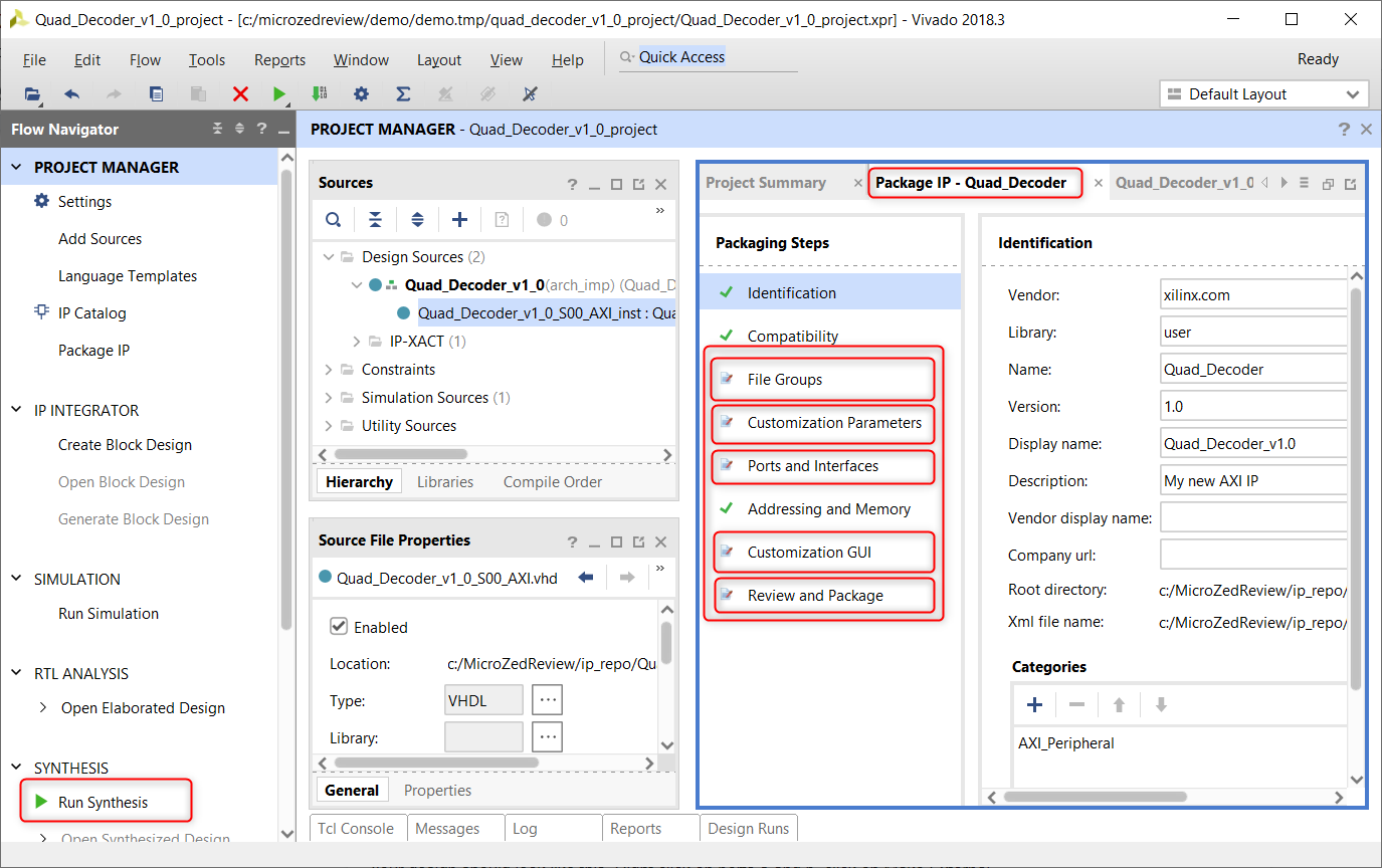
Now the IP module needs to be saved, click Run Synthesis, once synthesis is complete navigate to Package IP.
Click on each tab that needs changes, finally click on Repackage IP and close the project.
Add your new IP block to the block design, run block automation.
Your design should look like this. Right click on ports a and b, click on Make External
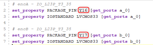
Right Click on Constraints, Add Sources. Follow the steps to create a new constraints file. Paste in the <QuadratureConstraints.xdc> file.
Change the pin numbers to match your I/O pin selection.
<QuadratureConstraints.xdc>
# encA - IO_L23P_T3_35
set_property PACKAGE_PIN Y16 [get_ports a_0]
set_property IOSTANDARD LVCMOS33 [get_ports a_0]


# encB - IO_L23P_T3_35
set_property PACKAGE_PIN Y17 [get_ports b_0]
set_property IOSTANDARD LVCMOS33 [get_ports b_0]
Follow steps 14 to 16 from the Hello World project to add the HDL wrapper, synthesise the project and export hardware.
Launch SDK, create an empty C project and also Create a C++ project.
Copy platform.c, platform.h and platform_config.h from the C project src folder into the C++ project src folder.
Paste <main.cc> code into your main.cc file.
<main.cc>
#include <stdio.h>
#include "platform.h"
#include "xparameters.h"
#include "stdlib.h"

struct Registers {
   uint32_t Direction_Reg; //
   uint32_t Flag_Reg; //
};

static Registers * const AXI = reinterpret_cast<Registers *>(XPAR_QUAD_DECODER_0_S00_AXI_BASEADDR);

int Direction;


int main(){
     init_platform();
     for(;;){
          if (AXI->Flag_Reg != 0){
               Direction = AXI->Direction_Reg;
               printf("Direction = %u \n", Direction);
          }
     }
     cleanup_platform();
     return 0;
}
The code works by continually polling the flag register. Once Flag_Reg is high, the value from the Direction_Reg is written to Direction variable.
Direction is printed to the terminal, Left = 0, Right = 1.
You may need to replace a section of the code shown above as XPAR_QUAD_DECODER_0_S00_AXI_BASEADDR with code specific to your project.
To do this, highlight the text "xparameters.h", press F3, this will open the xparameters header file.
Find the section that describes your custom IP block:

Delete the original C project.
Build, Program and run the project, the direction will be displayed in the terminal window:
Conclusion
The only other FPGA I have used recently is the Digilent Zybo. The MicroZed has a much smaller footprint and much more limited range of connectivity choices. It is ideal for projects that do not require pre existing audio/video interfaces (as is included on the Zybo). The Microzed is a better option for projects that require a greater number of I/O.


One thing that took quite a while to figure out was how to use configure the UART. When i tried to run the program in SDK, an error message said that there was no UART interface. This was solved by going back to Vivado, double clicking the Zynq IP and enabling the UART (as shown in step 13). When the Microzed was plugged into the carrier card, it was not allowing me to connect the terminal to the board. By plugging the Microzed into the carrier card, the power connection through the Microzed micro USB is disabled and it must also disable the UART. After some reading and trial and error, this was solved by changing the jumper configuration as shown below. With this configuration, the Microzed is powered from the expansion card micro USB and the UART still works though the MicroZed micro USB connector. This means 3 USB cables are required. It would be useful if it could be programmed over USB, but it’s not that much of an inconvenience.
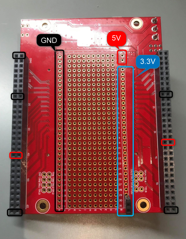
Whilst experimenting with the board, I required a 3.3V source for the encoder. There are two 5V and multiple ground connections located in the 60 pin connectors but no 3.3V connections. In order to source 3.3V I had to solder another connector on to the 3.3V rail in the centre of the carrier card.
Edit > [ the 3.3V line is available in the 60 pin connectors (labelled as VCCio, adjustable to 1.8, 2.5 or 3.3 V with the jumper next to the power switch) on pins 53 and 54 in connector 1 and pins 49 and 50 in connector 2].
In conclusion, I highly recommend this board to anyone that requires a versatile SoC/FPGA with a high number of I/O and a small footprint.


Future Work:
The MicroZed will be used to develop my final year project. I have built a prototyping board and will update this page in the coming months with information on progress.


Top Comments
Brenton,
I think this was your first roadtest review. A fine job. You caught my interest and walked me through your experience of the product quite well. thanks.
Randall Scasny
RoadTest Program Manager