RoadTest: Cmod S7: Breadboardable Spartan-7 FPGA Module
Author: davide.bellizia
Creation date:
Evaluation Type: Development Boards & Tools
Did you receive all parts the manufacturer stated would be included in the package?: True
What other parts do you consider comparable to this product?: The only thing that comes into my mind is the whole Digilent CMOD series, that they have more or less same features with diffirent FPGAs. Slightly more complete, another similar product is the Terasic DE0 Nano, that has more peripherals but it does not have the nice feature of being breadboardable-
What were the biggest problems encountered?: Due to COVID-19 restrictions I had some delay in receiving the package, and I could not use all the material I wanted to use initially, so I had to improvise a bit.
Detailed Review:
Introduction
This RoadTest has the aim of testing out the Digilent CMOD S7 evaluation-board, mounting the Xilinx Spartan-7 FPGA.
Unboxing
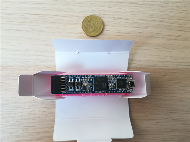
The product: Digilent CMOD S7
The package itself is very small, as the board, that has the nice feature to be easily integrated on a breadboard, or in general, on a DIP-40 2.54mm socket. The board is shipped with no cable, but they are quite common, and therefore it is not such a problem. It is noticeable the absence of any instruction manual and/or schematic, which are available directly on Digilent website along with schematics and other useful information.
The package and the board are shown below (0.50€ coin as reference).


The Board
The board is basically composed by:
As listed above, the board is very basic (and it explains its low price compared to other Digilent products) and thus, many features that FPGA users use to see on bigger boards, as SD-card dock, RAM memory, etc., are not available here.
The FPGA itself worth the money. I’ve used intensively Spartan-6 series, due to their reliability and cheap price, making them the perfect choice as controller for experimental ASICs and other bigger FPGA designs. The Spartan-7 inherits the good characteristics of its predecessor, taking advantage of all improvements Xilinx deployed on series7, for which, a 28nm process has been used to improve performance, reduce power and increase density.
Example of usage
Due to basic features that the board offers, I’ve been motivated in trying to design a post-apocalypse DSP (Digital Signal Processor) for electric guitar (it is one of my passion). My main objective has been to create a basic platform to test DSP algorithms using the minimal amount of component, and relying mostly on the features provided within the FPGA boundary. Of course, this little project does not aim to be hi-fi (at least in this primary version), but it will serve as a base to test some ideas that are ringing in my head since years.
The whole design is shown in a simplified form in the figure below, and it is composed by 3 essential blocks:

This minimal approach is essential devoted to the needs to have something to play with during the strict confinement that in Europe has been active during the spring time. Therefore, instead of using explicit ADC and DAC blocks, I have tried to use directly the resources I could take advantage on the FPGA. In fact, Xilinx Series-7 FPGA are equipped with an internal dual-channel ADC (called XADC in ISE/Vivado toolchains), which provides 12bits precision with a maximum 1MS/s. Clearly, 12bit precision are not that much for guitar, as commercial DSP units work usually with 24bits, that means much more information and accuracy (and less distortion). As I said, I wanted to have something really minimal, and for this V1 version, I could stand and accept the 12bit.
The first block of the design is, hence, the anti-alias filter, which for our application is as simple as a low-pass filter (LPF). For newbies, its role is to limit the bandwidth of the signal we provide to an ADC, in order to avoid aliasing due to violation of the Sampling Theorem, which would provide distortion and inaccuracy to our digital representation. The LPF filter as a Sallen-Key filter, adopting a single operation amplifier, with a cut-off frequency of 16kHz. In fact, consider that I’ve set the ADC inside the FPGA to capture the input signal with a sampling frequency of 44.1kHz. Hence, every frequency at half of this value has to be strongly attenuated in order to guarantee that no aliasing frequency components will be in our spectrum. Usually, the very top frequency for guitar is around 10-12kHz, so, setting the cut-off at 16kHz leaves us more margin and less noisy signal at the input of the ADC. As op-amp I’ve used two MCP6292 (dual op-amps with the same pinout of TL0x2, I have them lying around), that I powered at 3.3V from the PMOD connector of the CMOD board. I decided to not run it at 5V (also available on the UIN pin of the board) due to safety reasons. The XADC of the FPGA could get easily damaged if the range of the input signal exceed the reported and admitted value. Adopting 3.3V ensures that we can stay safely in the range, also according to the documentation of the Digilent board (there is a specific on-board attenuation network to tolerate 0 to 3.3V signals).
The main core of the DSP is indeed the Xilinx Spartan7 FPGA. I have used the internal PLL to increase a bit the system clock frequency, which basically means that we modify the clock provided by the on-board clock reference from 12MHz to 24MHz. The analog signal is sampled by the XADC, which provides a 12bit resolution. The XADC is set to provide a sampling rate that is very close to 44.1kHZ (which is very common for audio application). Of course, 16bit would have been much better for the signal-to-noise ratio (SNR), but for this “doomsday” multieffect we can admit and stay in the lo-fi zone. The digital signal processing part of the design is shown in the Figure above and it is composed by:
The UART interface receives 3 bytes for each message (not that far for MIDI, for which the conversion would require 10 minutes…), in order to change parameters and enable/disable modules. The information that the UART module receives are processed by the Controller unit, which routes the received bytes to the proper module.
The Distortion module is composed by 3 main blocks. A first one is a simple multiplier, which acts as a “preamp” stage. The second is a 5-segments piecewise linear approximation of a hyperbolic tangent operator, that is widely used as activation function for Neural Networks. This particular function (as well as the sigmoid) is very well suited for approximating the non linear behavior of overdrive and distortion units for guitar. An additional multiplier/amplifier stage is used to set the post-distortion volume.
The Delay module is the richest and bigger part of the design, implementing an echo (it is not that hi-fi) generator mimicking large room with several repetitions of the input signal. In fact, the module contains a delay line implemented as a dual-port RAM of 65536 16bit words, clocked at 44.1kHz. Hence, the total amount of delay we are able to generate is 1.48s. The entire RAM can be hosted on BRAM primitives of the FPGA, fulfilling the silent requirement of using the minimum number of components. This amount of delay takes 60% of the BRAM quantity available on this specific FPGA. Having two ports, one for writing the RAM and the other for reading, we can easily set the delay time as a difference between the writing address and the reading address of the memory, being sure of not creating any collision. To create a working delay, we also need to create a feedback path. Therefore, the delay as acoustic effect needs a feedback architecture to be effective, which is easy to implement through the classic Infinite Impulse Response (IIR) structure, widely use for digital filters. The input of delay line/RAM is fed by a sum of the input signal and a scaled version of the output of the delay line according to the amount of delay needed by the user. The scaling factor affects the number of repetitions, or, in other words, the energy of the repetition in the feedback path. Of course, if this factor is too high, the IIR structure will not be stable anymore, and, as side-effect, we can obtain infinite repetitions.
The additional feature of the Delay module is the presence of a tunable Low-Frequency Oscillator (LFO), that is particularly useful to create a chorus-y effect upon the delay (also known as modulated delay in the effect community). The LFO can be enable and its triangle wave oscillation frequency can be varied from 0.02Hz up to XXX Hz, through the dedicated serial message. In this configuration, the LFO modulate the delay time (which is a simple addition on the read pointer of the dual port RAM in the Delay module). As additional parameter, I decided to also add a “depth” control on the modulation, which amplifies the magnitude of the LFO wave to achieve a stronger/weaker chorus-y sound.
The final part of the digital chain is represented by the Digital-to-Analog (DAC) converter. While the Spartan7 on the Digilent CMOD S7 board has a nice dual channel ADC, it does not contain any DAC circuitry. To follow the rationale I explained in the beginning of this road-test’s report, I decided to implement a basic DAC upon the resources that the FPGA offers. In fact, a simple methodology to generate an analog signal from a digital word is to modulate the duty cycle of a fixed-frequency square wave, that basically requires a digital pin and a counter surrounded by some logic circuitry. With these simple amount of resources, we can create a so-called Pulse Width Modulation unit, that will encode the value of our processed samples into the duty cycle of a square wave, that can be easily processed by a low-pass filter and, thus, providing an analog representation of our digital data. This solution is quite popular among the Arduino community, and in general in several IoT applications, where there is no need of a super accurate DAC that would require more space on board and/or more power. At this stage, the design of the parameter that are involved in the PWM-based DAC conversion are several, and it does not exist a single way to achieve a certain level of accuracy. I decided to place two PWM units each of them working with a 24MHz input clock and 8bit counter, in order to achieve a decent accuracy. Using two PWM modulators requires two digital pins of the FPGA and an additional stage (implemented with two resistive trimmers) for having a weighted sum of the respective channel in order to balance the contribution of the two channels. In fact, one channel receive as input the most significant byte of our 16bit encoded digital data, while the other will receive the least significant one. The addition is performed using a summing opamp in non-inverting buffer mode, and an additional one is used to low-pass filter the signal, adopting again the Sallen-Key configuration with unity gain.
A simple and nice Python code handles the setting of the parameter by means of UART connection through the FT2232H FPGA. In the figure below, the very simple CLI interface (I am thinking to make a real GUI out of it with tkinter) I wrote is shown.
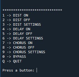
The code is very minimal and usually sends 3 bytes to the device, to tell, for example, which module has to be activated, what are the values and, of course, bypass the digital signal processing units singularly or as whole. In addition, three out of four green leds of the Digilent CMOS S7 board have been used as a simple an intuitive interface to show which module/submodule is enabled.
Finally, some overall impressions of the quality and future improvements are expressed as follows. The distortion module is very nice and sounds quite well without the needs of further digital low-pass filtering (usually needed to tame the fizzy residual of distortion and giving a more organic sound). The TanH trick to simulate an overdrive really did the job, and possibly, playing with approximation parameters one can obtain a more convincing outcome. The delay suffers from the lack of bits at the input XADC (consider that inside the FPGA, each interface is 16bit wide for signal), but it is functional and with the added LFO expands easily the sound palette, giving it a lo-fi 80s modulated delay. For this design, the resources I’ve used most is the BRAM for the delay unit (60% of the total), while the rest is basically still empty, and leave spaces for improvement and other modules. On my to do list there are a compressor, a dedicated flanger/chorus, tremolo (very easy with the LFO) and wha-wha. Clearly, in the next version I will try to avoid to use the XADC and PWM combo, and possibly using proper ADC and DAC to do this job. Already using a proper 16bit representation, would make me to gain theoretic 24dB of SNR at the input and many more at the output, avoid the distortion that the PWM modulation will inevitably provide.
Summary
In this RoadTest, the Digilent CMOD S7 has been tested and used to design a small multieffect for guitar. The board is very small and due to its simple form factor may be very attractive for people that want to add a real reconfigurable processor/accelerator for a nice price to their project. Being the price in the range of a Raspberry, it is not particularly cheap, but we must consider that this Digilent CMOD S7 contains a 28nm FPGA, that can host small CPU or deploy several peripherals as PLL, ADC and others. The form factor of the board makes it ideal for rapid prototyping on a breadboard (as I did for my project), and also good for switching devices for more advanced users/applications (e.g. testing inter-chip variation on several FPGAs for PUF/RNG testing).


Top Comments
Since you have experience with the tool set, how easy would this kit be to use by a newbie?
What minimum experience should someone have before they try to use it?
DAB