


If you have ever populated a PCB with lots of SMD components by hand, you know how frustrating and time-consuming it can be. Thankfully, when its time to move into production we employ special robots called “pick and place” machines to do the job for us, and while these robots are capable of placing very small components very accurately at an incredibly fast pace, they are still limited in how small the components it can place are. This has become an issue recently because as technology advances, the components that make up that tech shrink in size, and we are at a point that some discrete components have shrunk in size and are no longer visible without some heavy magnification.
“Electronics manufacturing requires handling and assembling small components in a size similar to or smaller than grains of flour,” says Sanha Kim, a former MIT postdoc and research scientist who worked in the lab of mechanical engineering associate professor John Hart. “So a special pick-and-place solution is needed, rather than simply miniaturizing [existing] robotic grippers and vacuum systems.”
A typical pick and place machine utilizes suction to pick up components and then place them in the correct location on a PCB, but the suction technique is only effective down to about 100-micron, beyond that, the force of gravity begins to outweigh force of the suction, and the parts simply fall off of the placement head. Recently a team of researchers from the Massachusetts Institute of Technology published a paper detailing a new method to pick up these microscopic components and place them accurately onto a substrate.
“The dominance of surface forces over gravity forces becomes a problem when trying to precisely place smaller things — which is the foundational process by which electronics are assembled into integrated systems,” Hart says.
This new method utilizes a special “electroadhesive” stamp that is built from what can best be described as a “forest” of carbon nanotubes that have been coated in a special ceramic material and creates something similar to a brush with millions of tiny bristles. When a voltage is applied to the stamp, the ceramic-coated carbon nanotubes develop a charge that is capable of attracting a microscopic component and holding it firmly enough to move it over to its position on the PCB. To release the component, the power to the stamp is turned off, and the carbon nanotubes lose their charge.
“Simply by controlling voltage, you can switch the surface from basically having zero adhesion to pulling on something so strongly, on a per unit area basis, that it can act somewhat like a gecko’s foot,” Hart says.
So just how small of an object can this new electroadhesive stamp pick up? The team says that at the moment the device is capable of picking up objects up to 20-microns in size, that’s 5-times smaller than a standard sheet of paper is thick. The team admits that this concept is similar to industrial processes used to move delicate objects such as thin textiles, and silicon wafers, but this process is the first time electroadhesion has been utilized at the microscopic level.
The team of researchers discovered this new process while working on carbon nanotubes as the basis for a dry adhesive. During this research, the team found that they could coat the carbon nanotubes in a thin dielectric material like aluminum oxide. When a voltage was applied, the ceramic layer became polarized. When the positively charged tip of one of the nanotubes came within close proximity of a small object, that object adopted a negative charge causing the object to become attracted to the nanotube. This attraction turned out to be strong enough to overcome the force of gravity and allowed the small object to remain “stuck” to the nanotube.
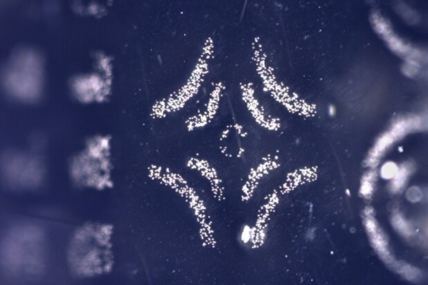
Interestingly enough, the team discovered that the density of the carbon nanotube forest, as well as ceramic layer thickness, greatly impacted the stamp’s “stickiness.” A thinner ceramic layer combined with a sparsely populated carbon nanotube forest produced the most attraction and holding power, while thicker ceramic and a very dense forest of nanotubes actually had the opposite effect.
“With ever-advancing capabilities of semiconductor devices, an important need and opportunity is to integrate smaller and more diverse components, such as microprocessors, sensors, and optical devices,” Hart says. “Often, these are necessarily made separately but must be integrated together to create next-generation electronic systems. Our technology possibly bridges the gap necessary for scalable, cost-effective assembly of these systems.”
Source: http://news.mit.edu/2019/electroadhesive-stamp-microscopic-manufacturing-1011
