


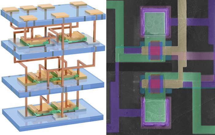
Schematic and false-colored electron microscopy of monolithic 3D SRAM cell. (Image Credit: University of Illinois Urbana-Champaign)
Researchers at the University of Illinois Urbana-Champaign created a new technique to produce 3D chips. They did this by vertically stacking ultrathin layers of silicon circuits without performance loss. According to the team, the monolithic 3D chip could extend Moore’s Law beyond traditional 2D scaling limits.
“Vertical integration is already starting to make its way into commercial devices, particularly in specialized AI hardware, but monolithic integration is what unlocks the full promise of 3D chips,” Illinois Grainger Engineering materials science and engineering professor Qing Cao said. “For the first time, we have met the thermal budget of monolithic 3D integration using standard single-crystalline silicon and delivered unprecedented performance.”
For a while, heat has been a technical challenge for 3D chips. Additional circuit layers must be integrated above completed wiring and devices without melting or degrading the layers underneath. To overcome this issue, the team used a low-temperature fabrication technique that relies on single-crystal silicon nanomembranes measuring 10 nanometers thick or less.
They created the silicon films separately and used a roll laminator to transfer them onto a substrate that has bottom-layer circuits. Temperatures only need to reach 392 F to produce a strong bond between the substrate and the transferred layer.
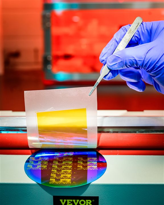
The team transfers the ultrathin silicon membrane onto the wafer. (Image Credit: University of Illinois Urbana-Champaign)
The team also used junctionless transistor designs to avoid high-temperature doping. Rather than using extreme heat to produce sharp p-n junctions, the team uniformly and heavily doped the silicon. With the ultrathin layers, the gate still controls current flow. Meanwhile, the high doping decreases parasitic contact resistance.
Even though these are fabricated at a low temperature, the transistors achieve current densities comparable to those produced at high temperatures. In addition, they perform three to four times better than low-temperature materials used in monolithic 3D schemes. Engineers can then stack high-performance transistors on circuitry without exposing the underlying layers to heat.
The researchers used this process to fabricate three vertically stacked silicon layers. Each layer has 625 transistors, achieving device yields of 98-100%. All the layers were connected using vertical metal interconnects, demonstrating reliable functionality for 3D logic circuits and SRAM cells. Some SRAM cells only took up 1/3rd of the area of similar 2D cells, showing the potential for significant density gains.
This technology may play a huge role in the future of computing. By vertically stacking transistors, signals travel less time between circuit blocks. It also reduces parasitic effects and increases bandwidth. These are beneficial for data-heavy applications like AI training and inference. Since this technique relies on single-crystal silicon and can be implemented in foundry processes, it could eventually be commercialized.
“But most importantly, we’ve shown that this process is scalable,” Cao said. “You can keep stacking layers beyond the three we demonstrated. And the process will yield high-performing transistors with high yield and low variability. We now have a strong foundation for transferring this technology and demonstrating its immediate promise in an industrial semiconductor foundry.”
Have a story tip? Message me here at element14.