element14 Community
element14 Community
    Register Log In
  • Site
  • Search
  • Log In Register
  • Community Hub
    Community Hub
    • What's New on element14
    • Feedback and Support
    • Benefits of Membership
    • Personal Blogs
    • Members Area
    • Achievement Levels
  • Learn
    Learn
    • Ask an Expert
    • eBooks
    • element14 presents
    • Learning Center
    • Tech Spotlight
    • STEM Academy
    • Webinars, Training and Events
    • Learning Groups
  • Technologies
    Technologies
    • 3D Printing
    • FPGA
    • Industrial Automation
    • Internet of Things
    • Power & Energy
    • Sensors
    • Technology Groups
  • Challenges & Projects
    Challenges & Projects
    • Design Challenges
    • element14 presents Projects
    • Project14
    • Arduino Projects
    • Raspberry Pi Projects
    • Project Groups
  • Products
    Products
    • Arduino
    • Avnet Boards Community
    • Dev Tools
    • Manufacturers
    • Multicomp Pro
    • Product Groups
    • Raspberry Pi
    • RoadTests & Reviews
  • Store
    Store
    • Visit Your Store
    • Choose another store...
      • Europe
      •  Austria (German)
      •  Belgium (Dutch, French)
      •  Bulgaria (Bulgarian)
      •  Czech Republic (Czech)
      •  Denmark (Danish)
      •  Estonia (Estonian)
      •  Finland (Finnish)
      •  France (French)
      •  Germany (German)
      •  Hungary (Hungarian)
      •  Ireland
      •  Israel
      •  Italy (Italian)
      •  Latvia (Latvian)
      •  
      •  Lithuania (Lithuanian)
      •  Netherlands (Dutch)
      •  Norway (Norwegian)
      •  Poland (Polish)
      •  Portugal (Portuguese)
      •  Romania (Romanian)
      •  Russia (Russian)
      •  Slovakia (Slovak)
      •  Slovenia (Slovenian)
      •  Spain (Spanish)
      •  Sweden (Swedish)
      •  Switzerland(German, French)
      •  Turkey (Turkish)
      •  United Kingdom
      • Asia Pacific
      •  Australia
      •  China
      •  Hong Kong
      •  India
      •  Korea (Korean)
      •  Malaysia
      •  New Zealand
      •  Philippines
      •  Singapore
      •  Taiwan
      •  Thailand (Thai)
      • Americas
      •  Brazil (Portuguese)
      •  Canada
      •  Mexico (Spanish)
      •  United States
      Can't find the country/region you're looking for? Visit our export site or find a local distributor.
  • Translate
  • Profile
  • Settings
Embedded and Microcontrollers
  • Technologies
  • More
Embedded and Microcontrollers
Blog Researchers discover new theory for semiconductors made of nanocrystals
  • Blog
  • Forum
  • Documents
  • Quiz
  • Polls
  • Files
  • Members
  • Mentions
  • Sub-Groups
  • Tags
  • More
  • Cancel
  • New
Join Embedded and Microcontrollers to participate - click to join for free!
  • Share
  • More
  • Cancel
Group Actions
  • Group RSS
  • More
  • Cancel
Engagement
  • Author Author: Catwell
  • Date Created: 7 Jul 2020 6:28 PM Date Created
  • Views 644 views
  • Likes 4 likes
  • Comments 1 comment
  • nanocrystals
  • on_campus
  • cabeatwell
  • electronics
  • university
  • innovation
Related
Recommended

Researchers discover new theory for semiconductors made of nanocrystals

Catwell
Catwell
7 Jul 2020

image

A new theory offers the first explanation for how electrical currents move throughout nanocrystals. The nanocrystal model developed by ETH researchers. (Image credit: ETH)


Researchers at ETH Zurich recently made a groundbreaking discovery about semiconductors made of nanocrystals. Theoretical understanding of how electrical current moves through nanocrystals eluded researchers up until now. The team has hit upon the first theoretical explanation for how electrical current is conducted in semiconductors made of nanocrystals.


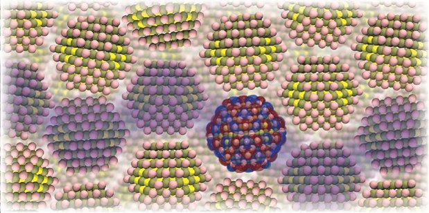
The method for how electric currents travel through semiconductors is well known. The electronic properties of semiconductors can be controlled by adding impurity atoms, which changes the number of electrons. However, semiconductors made of small nanocrystal quantum dots can’t change with these methods. Whereas currents move smoothly through typical semiconductors, currents sink and deform in nanocrystal material. Due to this, the team had to change how they looked at the atoms in the crystal lattice of the nanocrystal semiconductor


Researchers ran a complex code using the Swiss Supercomputing Center CSCS in Lugano to get a better understanding of how these charges move between nanocrystals and what prevents them from moving further. The results showed how material made of many nanocrystals conducts electrical current are small deformations of crystals that cause a huge change in electrostatic energy. The current flows through polarons – when a charge deforms the material around it – causing it to hop from one nanocrystal to the next.


The team then tested the theory using thin films of nanocrystal produced in the laboratory and measured the electric response for different applied voltages and temperatures. They created free electrons at one end of the material using a short laser pulse and noted when they arrived at the other end. The computer simulation accurately predicted the electrical properties during each test.


These results could be used to develop semiconductors from nanocrystals materials for various applications in sensors, lasers, or LEDs. These materials could lead to a much broader variety of electrical properties than normal semiconductors.


Have a story tip? Message me at: cabe(at)element14(dot)com

http://twitter.com/Cabe_Atwell

  • Sign in to reply
  • DAB
    DAB over 5 years ago

    They are still stuck with an outdated atomic model and the belief that an entire electron can be ripped from one atom to another.


    My photon transfer theory is much more elegant and preserves the atom at all phases.


    DAB

    • Cancel
    • Vote Up 0 Vote Down
    • Sign in to reply
    • More
    • Cancel
element14 Community

element14 is the first online community specifically for engineers. Connect with your peers and get expert answers to your questions.

  • Members
  • Learn
  • Technologies
  • Challenges & Projects
  • Products
  • Store
  • About Us
  • Feedback & Support
  • FAQs
  • Terms of Use
  • Privacy Policy
  • Legal and Copyright Notices
  • Sitemap
  • Cookies

An Avnet Company © 2025 Premier Farnell Limited. All Rights Reserved.

Premier Farnell Ltd, registered in England and Wales (no 00876412), registered office: Farnell House, Forge Lane, Leeds LS12 2NE.

ICP 备案号 10220084.

Follow element14

  • X
  • Facebook
  • linkedin
  • YouTube