element14 Community
element14 Community
    Register Log In
  • Site
  • Search
  • Log In Register
  • Community Hub
    Community Hub
    • What's New on element14
    • Feedback and Support
    • Benefits of Membership
    • Personal Blogs
    • Members Area
    • Achievement Levels
  • Learn
    Learn
    • Ask an Expert
    • eBooks
    • element14 presents
    • Learning Center
    • Tech Spotlight
    • STEM Academy
    • Webinars, Training and Events
    • Learning Groups
  • Technologies
    Technologies
    • 3D Printing
    • FPGA
    • Industrial Automation
    • Internet of Things
    • Power & Energy
    • Sensors
    • Technology Groups
  • Challenges & Projects
    Challenges & Projects
    • Design Challenges
    • element14 presents Projects
    • Project14
    • Arduino Projects
    • Raspberry Pi Projects
    • Project Groups
  • Products & Partners
    Products & Partners
    • Arduino
    • Avnet & Tria Boards Community
    • Dev Tools
    • Manufacturers
    • Multicomp Pro
    • Product Groups
    • Raspberry Pi
    • RoadTests & Reviews
  • About Us
    About the element14 Community
  • Store
    Store
    • Visit Your Store
    • Choose another store...
      • Europe
      •  Austria (German)
      •  Belgium (Dutch, French)
      •  Bulgaria (Bulgarian)
      •  Czech Republic (Czech)
      •  Denmark (Danish)
      •  Estonia (Estonian)
      •  Finland (Finnish)
      •  France (French)
      •  Germany (German)
      •  Hungary (Hungarian)
      •  Ireland
      •  Israel
      •  Italy (Italian)
      •  Latvia (Latvian)
      •  
      •  Lithuania (Lithuanian)
      •  Netherlands (Dutch)
      •  Norway (Norwegian)
      •  Poland (Polish)
      •  Portugal (Portuguese)
      •  Romania (Romanian)
      •  Russia (Russian)
      •  Slovakia (Slovak)
      •  Slovenia (Slovenian)
      •  Spain (Spanish)
      •  Sweden (Swedish)
      •  Switzerland(German, French)
      •  Turkey (Turkish)
      •  United Kingdom
      • Asia Pacific
      •  Australia
      •  China
      •  Hong Kong
      •  India
      •  Japan
      •  Korea (Korean)
      •  Malaysia
      •  New Zealand
      •  Philippines
      •  Singapore
      •  Taiwan
      •  Thailand (Thai)
      •  Vietnam
      • Americas
      •  Brazil (Portuguese)
      •  Canada
      •  Mexico (Spanish)
      •  United States
      Can't find the country/region you're looking for? Visit our export site or find a local distributor.
  • Translate
  • Profile
  • Settings
Embedded and Microcontrollers
  • Technologies
  • More
Embedded and Microcontrollers
Blog Researchers Expand Photonic Chip Capabilities by Stacking Tiny Crystal Films
  • Blog
  • Forum
  • Documents
  • Quiz
  • Polls
  • Files
  • Members
  • Mentions
  • Sub-Groups
  • Tags
  • More
  • Cancel
  • New
Join Embedded and Microcontrollers to participate - click to join for free!
  • Share
  • More
  • Cancel
Group Actions
  • Group RSS
  • More
  • Cancel
Engagement
  • Author Author: Catwell
  • Date Created: 21 Oct 2026 8:00 AM Date Created
  • Views 34 views
  • Likes 3 likes
  • Comments 0 comments
  • stacking
  • mit
  • epfl
  • silicon photonics
  • photonics
  • Washington University
  • alternative materials
  • university
Related
Recommended

Researchers Expand Photonic Chip Capabilities by Stacking Tiny Crystal Films

Catwell
Catwell
21 Oct 2026

image

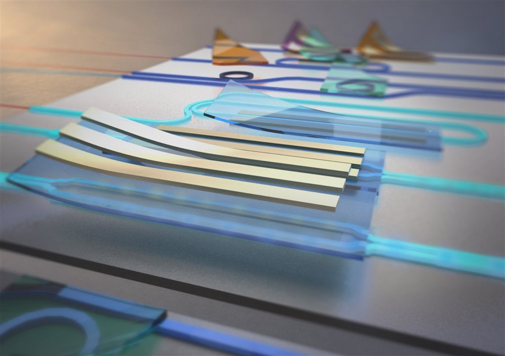
Render of 3D single-crystalline nanomembranes integrated on silicon photonics. (Image Credit: Wenbo Mao, Yuan Meng, Zhihao Xu, Di Jia

Photonic chips use light for information transmission and processing. Silicon and silicon nitride can guide light, but they don’t provide every optical function that advanced systems need. Researchers from Washington University, EPFL, and MIT integrated single-crystalline functional materials onto silicon and silicon nitride photonic chips. By doing so, photonic chips could offer more capabilities for computing and sensing.

Usually, integrating materials with different atomic structures on photonic chips can cause crystal defects to form. Those incompatibilities may worsen performance while limiting which materials can be combined. The team solved this issue by preparing crystalline materials on individual substrates and detaching them as nanomembranes (ultrathin layers). These layers are then placed on photonic chips, vertically stacked or laterally stitched.

Their technique uses van der Waals forces, allowing the layers to stick without the atomic alignment that crystal-growth methods rely on. This is very similar to LEGO brick stacking.

To demonstrate multiple optical functions, the researchers integrated materials into silicon and silicon nitride photonic platforms. They used barium titanate to achieve electro-optic modulation so that electrical signals could control light. In a device, the half-wave voltage-length product reached 0.29 V-cm. Another one exhibited an electro-optic bandwidth that surpassed 23 GHz. Gallium arsenide and gallium nitride were also integrated into silicon nitride chips. This demonstrated photodetection across a range extending from near-ultraviolet to near-infrared wavelengths.

The team also conducted another experiment in which they combined cobalt ferrite with silicon microring resonators, enabling the magneto-optical control of light. That material supported nonreciprocal optical transmission, so that light behaves differently based on the direction it travels. Afterward, the team stacked barium titanate and cobalt ferrite above a silicon microring resonator. That device achieved electrical and magnetic control of light in the same structure.

The researchers tested their method with different crystalline materials, such as barium titanate films that were up to one inch across. Applications include data storage, sensing, photonic computing, optical communications, and quantum technologies. More tests need to be done to see how it can be used for large-scale use.

Have a story tip? Message me here at element14.

  • Sign in to reply
element14 Community

element14 is the first online community specifically for engineers. Connect with your peers and get expert answers to your questions.

  • Members
  • Learn
  • Technologies
  • Challenges & Projects
  • Products
  • Store
  • About Us
  • Feedback & Support
  • FAQs
  • Terms of Use
  • Privacy Policy
  • Legal and Copyright Notices
  • Sitemap
  • Cookies

An Avnet Company © 2026 Premier Farnell Limited. All Rights Reserved.

Premier Farnell Ltd, registered in England and Wales (no 00876412), registered office: Farnell House, Forge Lane, Leeds LS12 2NE.

Follow element14

  • X
  • Facebook
  • linkedin
  • YouTube