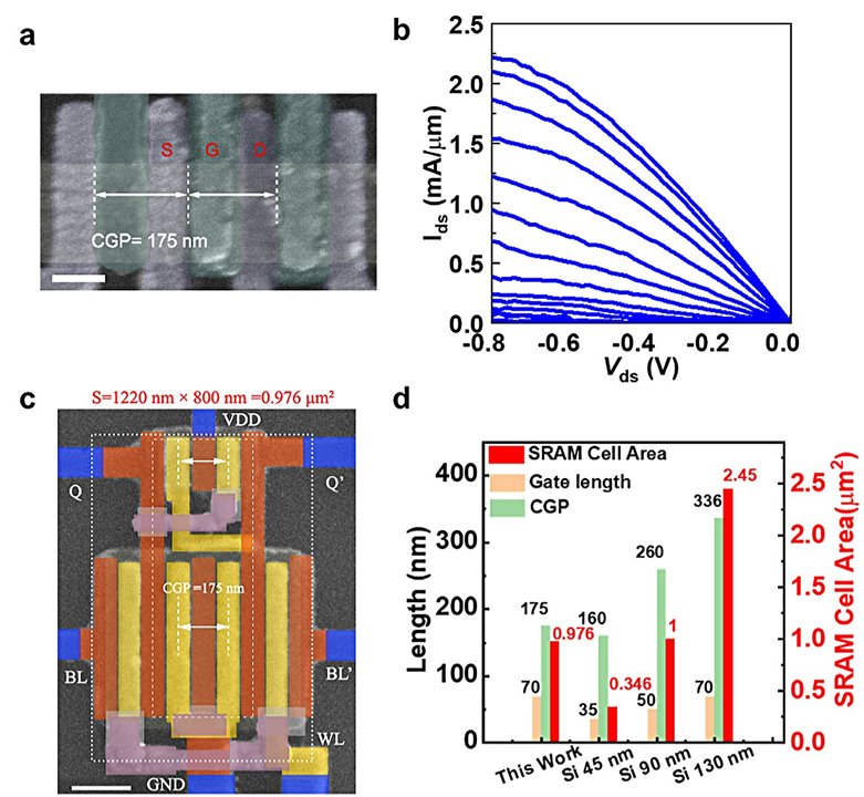
a) Carbon nanotube transistors based on nanotube arrays with a 175nm contacted gate pitch. B) Carbon nanotubes; output characteristics. c) A 6T-SRAM cell false-color image. d) Benchmark results for the 6T-SRAM cell with silicon technology nodes. (Image Credit: Lin et. Al.)
Electrical engineers have considered carbon nanotubes to be used in FETs for higher energy efficiencies, faster switching, lower leakage, and better performance. Researchers from Peking University and other institutes in China claimed they have realized that carbon nanotube-based FETs can be scaled down to the same density as 10nm semiconductor nodes. This work could make China’s manufacturing technology more modernized, keeping it guarded against US sanctions.
They say that progress toward achieving wafer-scale high-density semiconducting carbon nanotube arrays brought them a step closer to using carbon nanotubes in CMOS circuits. Even then, previous works involved scaling the channel or gate length of carbon nanotube transistors while maintaining large contact dimensions that don’t have applications for high-density CMOS circuits.

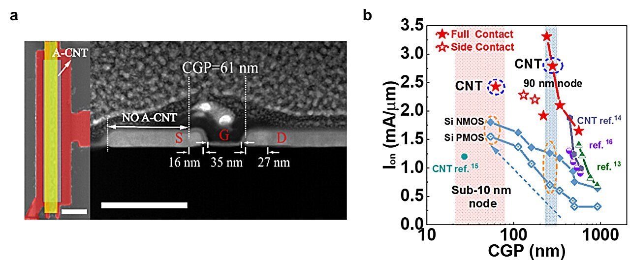
a) carbon nanotube transistor SEM and cross-sectional TEM image. b) Comparing the Ion at contacted gate pitch for carbon nanotube FETs in this study with other carbon nanotubes and silicon technology. (Image Credit: Lin et. Al.)
The team demonstrated the carbon nanotube transistors’ use and discovered they perform better than standard silicon-based FETs featuring a comparable gate pitch and a 6T SRAM cell area. They created carbon-nanotube-based FETs that have a 175nm contacted gate pitch, formed by scaling the contact length and gate length to 80nm and 85nm. As a result, the team claims it showed a 2.24 mA/um on-current and a 1.64 mS/um transconductance, exceeding the silicon 45 nm node transistors’ electronic performance. They also went on to say that a 90nm carbon nanotube node was achieved that can be scaled down and perform better than silicon 90nm node transistors.
Previous work demonstrated that charge carriers are only injected from the carbon nanotubes’ surface via side contact. This limits how much they can be scaled down because it evidently causes the resistance of the nanotubes’ length to become dependent. So the researchers formed a new scheme called full contact, which involves shortening each end of the carbon nanotube, making it possible to inject a portion of charge carriers from those regions.
As a result, carbon nanotubes can be miniaturized to contacted gate pitch below 55 nm corresponding to silicon 10 nm nodes. These also perform better than 10 nm node silicon transistors since they have high carrier mobility and Fermi velocity. The team’s work could eventually lead to the development of smaller and more efficient carbon nanotube-based transistors, which could prove very valuable for developing electronics.
Have a story tip? Message me at: http://twitter.com/Cabe_Atwell
