element14 Community
element14 Community
    Register Log In
  • Site
  • Search
  • Log In Register
  • Community Hub
    Community Hub
    • What's New on element14
    • Feedback and Support
    • Benefits of Membership
    • Personal Blogs
    • Members Area
    • Achievement Levels
  • Learn
    Learn
    • Ask an Expert
    • eBooks
    • element14 presents
    • Learning Center
    • Tech Spotlight
    • STEM Academy
    • Webinars, Training and Events
    • Learning Groups
  • Technologies
    Technologies
    • 3D Printing
    • FPGA
    • Industrial Automation
    • Internet of Things
    • Power & Energy
    • Sensors
    • Technology Groups
  • Challenges & Projects
    Challenges & Projects
    • Design Challenges
    • element14 presents Projects
    • Project14
    • Arduino Projects
    • Raspberry Pi Projects
    • Project Groups
  • Products
    Products
    • Arduino
    • Avnet Boards Community
    • Dev Tools
    • Manufacturers
    • Multicomp Pro
    • Product Groups
    • Raspberry Pi
    • RoadTests & Reviews
  • Store
    Store
    • Visit Your Store
    • Choose another store...
      • Europe
      •  Austria (German)
      •  Belgium (Dutch, French)
      •  Bulgaria (Bulgarian)
      •  Czech Republic (Czech)
      •  Denmark (Danish)
      •  Estonia (Estonian)
      •  Finland (Finnish)
      •  France (French)
      •  Germany (German)
      •  Hungary (Hungarian)
      •  Ireland
      •  Israel
      •  Italy (Italian)
      •  Latvia (Latvian)
      •  
      •  Lithuania (Lithuanian)
      •  Netherlands (Dutch)
      •  Norway (Norwegian)
      •  Poland (Polish)
      •  Portugal (Portuguese)
      •  Romania (Romanian)
      •  Russia (Russian)
      •  Slovakia (Slovak)
      •  Slovenia (Slovenian)
      •  Spain (Spanish)
      •  Sweden (Swedish)
      •  Switzerland(German, French)
      •  Turkey (Turkish)
      •  United Kingdom
      • Asia Pacific
      •  Australia
      •  China
      •  Hong Kong
      •  India
      •  Korea (Korean)
      •  Malaysia
      •  New Zealand
      •  Philippines
      •  Singapore
      •  Taiwan
      •  Thailand (Thai)
      • Americas
      •  Brazil (Portuguese)
      •  Canada
      •  Mexico (Spanish)
      •  United States
      Can't find the country/region you're looking for? Visit our export site or find a local distributor.
  • Translate
  • Profile
  • Settings
Embedded and Microcontrollers
  • Technologies
  • More
Embedded and Microcontrollers
Blog TSMC Reportedly Developing Rectangular Substrates for AI Applications
  • Blog
  • Forum
  • Documents
  • Quiz
  • Polls
  • Files
  • Members
  • Mentions
  • Sub-Groups
  • Tags
  • More
  • Cancel
  • New
Embedded and Microcontrollers requires membership for participation - click to join
  • Share
  • More
  • Cancel
Group Actions
  • Group RSS
  • More
  • Cancel
Engagement
  • Author Author: Catwell
  • Date Created: 30 Aug 2024 2:11 PM Date Created
  • Views 936 views
  • Likes 7 likes
  • Comments 0 comments
  • substrate
  • chip
  • manufacturing
  • pcb
  • cabeatwell
  • tsmc
  • innovation
Related
Recommended

TSMC Reportedly Developing Rectangular Substrates for AI Applications

Catwell
Catwell
30 Aug 2024

image

The rectangular substrates provide 3.7x more usable area than 300mm (12-inch) round wafers. (Image credit: TSMC via LinkedIn)

TSMC (Taiwan Semiconductor Manufacturing Co) is reportedly developing rectangular substrates for AI applications, according to an article from Nikkei. The development is still in its early stages and could take several more years before it's fully realized. That said, if the company manages to commercialize the technology, it could revolutionize the chip-making industry.

Instead of traditional 300mm diameter wafers, TSMC's new method of manufacturing rectangular substrates will boost that area up to 510mm by 515mm, providing 3.7 times more increased space. This would effectively allow for more chips to be produced from a single wafer, reducing the waste found on circular wafers. As with any innovative process, there are drawbacks, with the most notable being the need for new equipment. TSMC admits it can't use traditional fabrication tools for the new process; however the company is reportedly working with equipment and material suppliers, but the details are scarce.

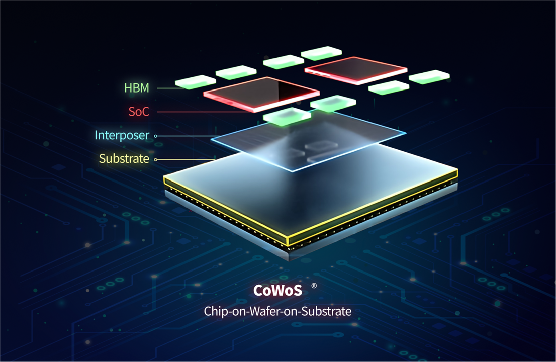
TSMC mentioned that it's closely following advancements in next-gen packaging technologies, including panel-level packaging. Once regarded as less advanced, chip packaging has now become a key factor in driving semiconductor innovation. For example, Nvidia's AI computing chips, such as the H200 and B200, rely on TSMC's 300mm CoWoS technology, which is crucial for manufacturing processors for faster data processing.

As AI chips grow in size and complexity, the efficiency of traditional manufacturing methods will decline, prompting the need for TSMC's rectangular wafers. Pushing toward those rectangular substrates is considered a long-term plan and will likely take five to ten years before becoming commercialized, as manufacturing equipment will need to be overhauled to accommodate the new shape and ensure the success of the new packaging method.

Have a story tip? Message me at: http://twitter.com/Cabe_Atwell

  • Sign in to reply
element14 Community

element14 is the first online community specifically for engineers. Connect with your peers and get expert answers to your questions.

  • Members
  • Learn
  • Technologies
  • Challenges & Projects
  • Products
  • Store
  • About Us
  • Feedback & Support
  • FAQs
  • Terms of Use
  • Privacy Policy
  • Legal and Copyright Notices
  • Sitemap
  • Cookies

An Avnet Company © 2025 Premier Farnell Limited. All Rights Reserved.

Premier Farnell Ltd, registered in England and Wales (no 00876412), registered office: Farnell House, Forge Lane, Leeds LS12 2NE.

ICP 备案号 10220084.

Follow element14

  • X
  • Facebook
  • linkedin
  • YouTube