


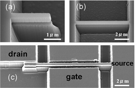
Scientists from the National Institute for Materials Science have succeeded in the batch fabrication of suspended structures of single crystal diamond for nano/micro electromechanical systems. The NEMS switch has the advantages of low-leakage current, low-power consumption and sharp on/off ratio in comparison with the conventional semiconductor devices. The NIMS research team, headed by Dr. Meiyong Liao, developed a process for fabricating suspended single crystal diamond structures by locally forming a graphite sacrificial layer in a single crystal diamond substrate by high energy ion implantation, followed by the growth of a diamond epilayer with electrical conductivity by microwave plasma chemical vapor deposition method (MPCVD) and the removal of the graphite sacrificial layer. The group also succeeded for the first time in fabricating NEMS switching devices with a transistor-like structure comprising 3 electrodes. The leakage current of the developed diamond NEMS switch is very low, and the power consumption is less than 10pW (picowatt). The devices exhibit high reproducibility, high reliability and no surface stiction. Stable operation of the diamond NEMS switch in a high temperature environment (250°C) was also confirmed. The Young’s modulus of the moveable cantilever structure was measured to be 1100GPa, which is close to the value of bulk diamond single crystals. Thus, high-speed (gigahertz) switching operation can be expected. For more information about diamond switch please visit: http://www.nims.go.jp/eng/news/press/2010/10/p201010140.html
Zero