

I m writing the issue observations in a clear and structured manner given below:
1. We have interconnected EVAL-AD9984AEBZ board with our test bench as given below:
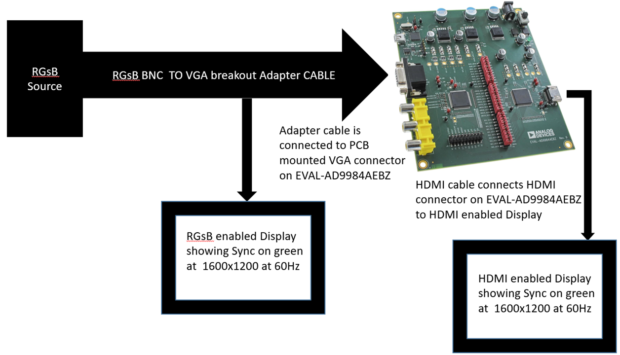
2. We first switch "ON" RGsB video generator source. Then changed the settings on VESA complaint Sync on Green Analog signal with 1600x1200 pixels at 60 Hz.
3. We checked RGsB display, if this display is working correctly. We found that above shown RGsB Display was actually showing Sync on green signal. Now, we can actually change the resolution of Sync on green video signal.
4. We connected EVAL-AD9984AEBZ to CPU using USB cable provided -> this made USB PWR LED (D7) glow onboard & switch "ON" the EVAL-AD9984AEBZ board using AC to DC adapter provided with board -> this made main power LED (D6) glow on board.
5. Now, we loaded AVES Blue & selected the connection tab. Thereafter, double clicked on CY7C68013 which actually connect this board with Windows based PC.
6. We added "AD9984A-VER.1.0c.txt" script in AVES Blue which gives us the options given below:
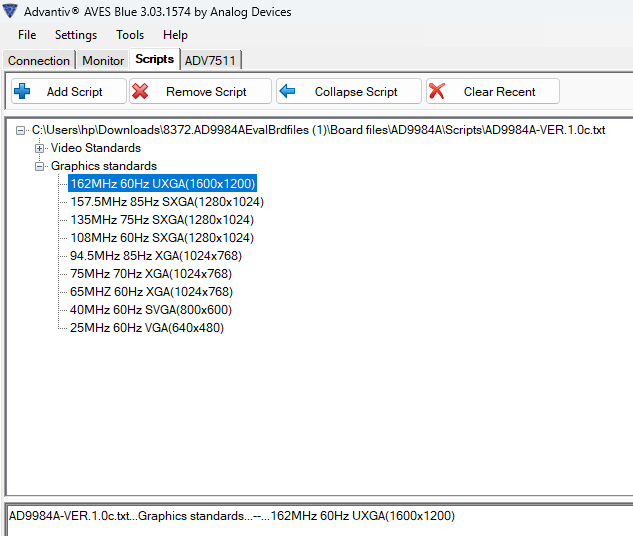
Out of these, we have selected "162MHz 60Hz UXGA(1600x1200)". Now, this settings will load default settings for AD9984A & ADV7511 as recommended by ADI.
Now, HDMI Display connected with this evaluation board gets refresh just for second & then goes into sleep mode displaying nothing at all.
Upon loading AD9984.xml file in AVESBlue, we get these answers on loading settings from AD9984 given below:
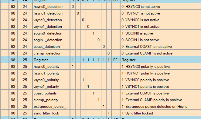
PLL of AD9984 is getting locked can be seen in above screenshot.
Please note: Given below procedure is not written in the documentation of EVAL-AD9984AEBZ but still we have managed to monitor the functioning of ADV7511.
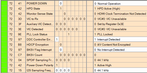
Upon loading ADV7511.xml file in AVESBlue, we get these answers on loading default settings from ADV7511 given below:

PLL of ADV7511 is not getting locked can be seen in above screenshot.
Since PLL of ADV7511 is not getting locked, there is no picture on HDMI output.
these are default settings given by Analog Devices:
98 00 01 ; Chip revision
98 01 87 ; PLL Div
98 02 00 ; PLL Div
98 03 F0 ; VCO range, Charge pump current
98 04 E0 ; VCO range, Charge pump current
98 05 00 ; Red Gain
98 06 80 ; Red Gain
98 07 00 ; Green Gain
98 08 80 ; Green Gain
98 09 00 ; Blue gain
98 0A 80 ; Blue gain
98 0B 00 ; Red offset
98 0C 80 ; Red offset
98 0D 00 ; Green offset
98 0E 80 ; Green offset
98 0F 00 ; Blue offset
98 10 80 ; Blue offset
98 11 20 ; Sync separator
98 12 00 ; Hsync
98 13 20 ; Hsync duration
98 14 04 ; Vsync
98 15 0A ; Vsync duration
98 16 04 ; precoset
98 17 04 ; postcoast
98 18 00 ; clamping
98 19 08 ; clamp placement
98 1A 14 ; clamp duration
98 1B 33 ; clamp polarity
98 1C FF ; ADI recommended write
98 1D 78 ; sync on green
98 1E 34 ; Input channel select
98 1F 93 ; Output video mode
98 20 07 ; Output impedance
98 21 20 ; ADI recommended write
98 22 32 ; ADI recommended write
98 23 14 ; sync filter window width
98 24 A8 ; sync detect
98 25 FD ; sync polarity
98 26 4E ; Hsync per vsync
98 27 20 ; Hsync per vsync
98 28 8F ; ADI recommended write
98 29 02 ; ADI recommended write
98 2A 00 ; ADI recommended write
98 2B 00 ; ADI recommended write
98 2C 00 ; ADI recommended write
98 2D 08 ; ADI recommended write
98 2E 20 ; ADI recommended write
98 3C 0E ; Auto gain
72 01 00 ; Set 'N' value at 6144
72 02 18 ; Set 'N' value at 6144
72 03 00 ; Set 'N' value at 6144
72 15 00 ; 24-bit, 444 RGB input
72 16 50 ; RGB
72 18 08 ; Disable CSC
72 17 01 ; Enable DE Generation
72 35 7B ; DE Generation
72 36 F0 ; DE Generation
72 37 0C ; DE Generation
72 38 80 ; DE Generation
72 39 4B ; DE Generation
72 3A 00 ; DE Generation
72 3B 40 ; Set Pixel Repetition
72 3C 00 ; Set VIC
72 40 80 ; General control packet enable
72 41 10 ; Power down control
72 49 A8 ; Set dither mode - 12-to-10 bit
72 4C 05 ; Set 10 bit output
72 96 20 ; HPD interrupt clear
72 55 00 ; Set to RGB
72 56 08 ; Set active format aspect
72 98 03 ; ADI recommended write
72 99 02 ; ADI recommended write - lock count limit
72 9C 30 ; PLL filter R1 value
72 9D 61 ; Set clock divide
72 A2 A4 ; ADI recommended write
72 A3 A4 ; ADI recommended write
72 AF 16 ; Select HDMI mode
72 BA A0 ; Set TX Clock Delay
72 DE 9C ; ADI recommended write
72 E4 60 ; VCO_Swing_Reference_Voltage
72 FA 7D ; Nbr of times to look for good phase
72 48 00 ; Evenly distrubuted output
72 55 10 ; RGB out
72 56 00 ; Set AVI
72 57 00 ; Adobe RGB
While debugging the reasons of misbehaviour of this board, we found that HSOUT,VSOUT & DATACK output from AD9984a was not compliant as per standard VESA timing for 1600x1200 pixel at 60 Hz sync on green with help of good quality 350MHz oscilloscope. These 3 signals were not stable, there was jitter in all 3 signals.
So, we decided to stabilized the waveform by changing the settings of following registers:
CHIP REGISTER SETTINGS
AD9984A 0x12 0x48
AD9984A 0x13 0xC0
AD9984A 0x14 0x0C
AD9984A 0x1D 0xB8
AD9984A 0x34 0xB4
ADV7511 0x41 0x00
These settings stabilized all 3 signals as per VESA timing standards for 1600x1200 pixel at 60Hz SoG.
We were able to secure the PLL lock of ADV7511 as result of above settings as per screenshot given below:
but still there was no picture output on HDMI Display shown above.
Now, I sincerely think that all of whom are accessing this, should be able to understand the how we are able reproduce the failure of this board.
if experts are able to understand this procedure ?
Kindly! help on urgent basis as this is critical problem. Since i m not getting any support.
THANKS WITH REGARDS
NEERAJ GUPTA