A printed circuit board (PCB) is the backbone of almost every electronic device. A well-designed PCB provides signal integrity, reduces production costs, reduces issues related to noise and heat, and improves a circuit's performance. This guide covers the details behind manufacturing, designing, and cleaning PCBs with an emphasis on the PCB’s connectors.
What is a PCB?
A printed circuit board (PCB) is a flat board that supports and electrically connects electronic components. A PCB is made of non-conductive material, typically fiberglass or a similar substrate. They have conductive traces, typically made of copper, that are etched or printed onto the board's surface. Components such as integrated circuits, magnetic components, resistors, capacitors, and connectors are mounted on the PCB, and the traces enable electrical signals to flow between them.
Types of PCBs
PCBs can be classified into several types based on various parameters.
Type of mounting
- Through-hole PCBs have holes drilled through the board, allowing the leads of electronic components to be inserted and soldered in. Through-hole PCBs are designed for DIP-based ICs and components with leads.
- Surface Mounted PCBs allow electronic components to be mounted directly on the surface. Unlike through-hole components, surface-mount components do not have wire leads. Instead, they have relatively small, flat metal contacts on their undersides, soldered directly on top of pads. Surface-mount components are much smaller than through-hole components, enabling much denser designs.
Number of layers
- Single-Layer PCBs have a single layer of copper traces on one side of the board. They usually have fewer components and can be easily manufactured.
- Double-Layer PCBs have copper traces on both sides of the insulating substrate. Compared to single-layer PCBs, their circuitry is typically more complex.
- Multilayer PCBs have three or more layers of copper traces separated by insulating layers. Multilayer PCBs support highly complex circuit designs.
Flexibility
- Rigid PCBs are made from material that maintains a fixed, inflexible shape. Rigid PCBs typically comprise layers of fiberglass-reinforced epoxy laminate, a non-conductive substrate.
- Flexible PCBs (Flex PCBs) are designed to be bendable and conform to the shape of the installed device. A Flex PCB uses flexible plastic material such as polyamide, polyether ether ketone, or transparent conductive polyester film as substrate. They are often used in wearable technology and curved displays.
- Rigid-Flex PCBs combine rigid and flexible sections within the same board. They are used in devices that require both flexibility and structural rigidity, such as foldable smartphones or aerospace applications.
The Different Parts of a PCB
The following are some of the parts that make up a PCB:
- Traces: Traces are conductive pathways, typically made of copper, that connect and carry electrical signals between components. Traces are created by chemically etching away the unwanted copper on a copper-clad PCB substrate, leaving behind the desired conductive paths in a specific pattern. Traces can also be created via PCB milling or printing.
- Pad: A pad is a flat metal area that serves as a connection point for electronic components. Pads are used to attach and solder components, such as resistors, capacitors, integrated circuits, and other electrical parts to the PCB. Pads provide the interface for electrical connections between the components and the board's circuitry. The size, shape, and arrangement of pads can vary depending on the specific requirements of the PCB and the components being used.
- Mounting Hole (Tool Hole): A hole that allows the circuit board to be connected to either a test fixture or its operational location.
- Copper Pour: A copper pour refers to a large area of the PCB's surface where copper is intentionally connected to create a solid, continuous, and usually unbroken plane of copper. This copper plane is typically used as a ground plane or a power plane, and it is used to provide a stable and low-impedance connection for electrical signals.
- Vias: Small holes or openings in a PCB that allow electrical connections to pass from one layer to another.
- Silkscreen: Also known as the solder mask, a silkscreen is a layer of printed information or markings on a PCB that is usually added to assist with component placement, identification, and assembly during the manufacturing and assembly processes.
- Annular Rings: The ring-shaped copper area surrounding a hole, such as a via or a through-hole. The primary function of the annular rings is to establish a robust electrical connection between a particular hole and a copper trace.
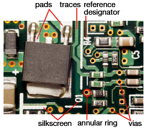
Figure 1: The Different Parts of a PCB
What is the Difference Between Blind Vias and Buried Vias?
A blind via is a type of hole or opening in a PCB that connects the outermost layers of a PCB to one or more internal layers but does not pass through the entire thickness of the board. Blind vias are used to create connections between the outer layers and inner layers of a multilayer PCB, allowing traces or signals to be routed to or from the inner layers without affecting the PCB's top or bottom surface. This design technique is often employed in high-density and compact PCB layouts to save space on the outer layers for surface-mounted components and routing.
A buried via is a type of via used in PCB design that does not extend to the outermost layers of the board. Designers utilize buried vias to create more complex and dense PCB designs. Buried vias can reduce signal interference and improve signal integrity.
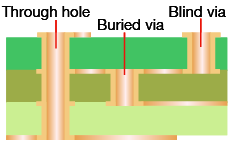
Figure 2: Blind and Buried Vias
What Materials are Used to Fabricate PCBs?
The following materials are used to fabricate PCBs:
FR-4 (Flame Retardant 4) is a widely used material in PCB manufacturing. FR-4 is a glass-reinforced epoxy laminate sheet known for its durability and electrical insulation properties. This material is flame-retardant, water resistant, and offers an excellent strength-to-weight ratio.
PTFE (Teflon) is a special plastic with minimal resistance and is frequently used for high-speed and high-frequency applications. PTFE is also lightweight and flame resistant, as well as exhibits high physical strength and temperature stability.
Metal: Traditional materials like copper, aluminum, iron, etc., are also used in PCB manufacturing. These materials allow component integration through Surface Mount Technology (SMT).
How to Manually Create a PCB
To manually create a PCBs, the following steps are necessary:
- Design the PCB layout: There are several software packages available for PCB design, including KiCad, Altium, and Proteus. The design process includes schematic creation, defining the components, and arranging the components on the board.
- Select a substrate material: These are often PTFE, FR-4, or metal.
- Transfer the layout: Print or draw the PCB layout onto transfer paper. Transfer paper is not paper in the traditional sense, but rather a type of thin, heat-resistant film or paper that allows you to transfer a printed circuit design onto a copper-clad board. This transfer process is commonly used in the "toner transfer method" for creating PCBs at home or in small-scale PCB prototyping.
- Prepare the PCB: Clean the PCB substrate to remove contaminants or residues, ensuring the copper surface is clean and free from oxidation.
- Transfer the design: Place the printed design onto the clean copper surface of the PCB and apply heat and pressure to transfer the toner or ink from the paper onto the copper, creating a resist pattern.
- Etch the PCB: Immerse the PCB in an etching solution (usually ferric chloride or ammonium persulfate) to remove the exposed copper not protected by the resist pattern, leaving behind the copper traces and pads according to the PCB layout.
- Remove the resist material: Remove the resist material from the PCB after etching. Use an appropriate solvent or a scrubbing process for this purpose.
- Drill holes: Use a drill press to make mounting holes (vias) where components are required and to connect traces between layers (if a multilayer PCB is used).
PCB Fabrication
When sending a PCB design out for fabrication, complete the following steps:
- Prepare the PCB layout for fabrication: Use PCB design or CAD software to design a circuit layout, considering factors such as placement of components, line laying, and board dimensions. Once you complete the PCB layout, export it into a format a PCB manufacturer can use. The most common format is the Gerber file, which contains all the necessary information for the manufacturer to create the PCB.
- Etch the PCB: After receiving the Gerber files, the manufacturer will create the PCB by printing the layout onto a copper-clad board and then etching away the unwanted copper. Similar to the previously discussed manual process, a chemical solution is applied to the board, which removes the copper not covered by the printed layout. The remaining copper forms the wires and pads that are used to connect the components.
- Drill the PCB: Once you receive the etched PCB, it is essential to drill holes for the components and mounting points. You may opt to use a computer-controlled drill bit to ensure accuracy and consistency. Once the holes have been drilled in the PCB, it should be ready for assembly.
What is the difference between PCB fabrication and PCB assembly?
PCB fabrication includes designing and creating the circuit board, while PCB assembly transforms a bare PCB into a functional unit, with components being soldered onto the board.
How to Order Custom-made PCBs
When ordering a fabricated PCB, the customer must provide the manufacturer with Gerber files generated by the PCB design software. However, the customer must also provide a Bill of Materials (BOM) enumerating all the necessary components and a pick-and-place file (often referred to as a “PnP file”) specifying each component's exact position for the PCB assembly process. These files are essential for configuring the automated soldering equipment.
What software do I need to design a PCB?
Some of the most popular PCB design software packages include:
- Altium Designer
- Autodesk EAGLE
- Cadence Allegro
- Proteus
- KiCad EDA
- Cadstar
- Sprint-Layout
- Mentor Graphics PADS
- Solidworks
- NI Multisim
- EasyEDA
Important Considerations in PCB Design
There are a few things to be aware of when creating a PCB design:
- Conceptualization: Define the functions of the PCB, its connections to other circuits, placement within the final product, and overall dimensions.
- Circuit Schematic: The circuit schematic includes all the necessary information for the board's electrical components to function correctly. Additionally, it should include a BOM for all the components needed for the PCB.
- PCB Mechanical Constraints: The designer should clearly define any mechanical constraints, such as board dimensions, thickness, cutouts, mounting holes, keep-out areas, mating interfaces, and locations of input/output connectors.
- Component Placement: The components must be placed correctly to establish solid electrical connections between circuits. Good placement ensures efficient assembly and successful testing of the PCB.
- Routing: The routing phase involves creating copper traces on the PCB layout, allowing the components to be interconnected.
- Validation: Validation encompasses the simulation and analysis of the PCB design to assess its functionality, ensure signal integrity, and evaluate thermal performance.
What are the different types of PCB connectors?
The different types of PCB connectors are:
Board-to-board connectors: Board-to-board connectors connect two PCBs to each other without a cable. They save space on cables, making them suitable for systems with limited space.
Wire-to-wire or cable-to-cable connectors: Wire-to-wire connectors are designed to join two or more separate electrical wires together, allowing for the transmission of electrical signals or power between them. They consist of contact points, or terminals, that are designed to accept and hold the stripped ends of wires.
Cable/wire-to-board connectors: Cable-to-board connectors connect a wire or cable to a board. Wire-to-board connectors commonly employ crimp technology to establish a connection between a wire and a PCB. After crimping the connector onto the wire, the terminals or contacts can be inserted into the appropriate housing to complete the interconnection.
How are Components Soldered onto PCBs?
The following soldering process is used for PCBs:
Wave Soldering: Wave soldering is a soldering process used in the mass production of printed circuit boards (PCBs) and electronic assemblies. It is particularly suitable for through-hole components. The wave soldering process involves the following steps:
- Flux Application: The first step is the application of flux to the PCB. Flux is a chemical agent that helps remove oxides from the metal surfaces (both the components and the PCB) and promotes good solder wetting. This ensures that the solder adheres properly to the metal surfaces.
- Preheating: The PCB with its components is passed through a preheating zone to gradually warm up the assembly. This helps in the evaporation of the solvent in the flux, reducing the risk of thermal shock during soldering.
- Solder Wave: The key step in wave soldering is the creation of a "solder wave." A molten solder (usually a tin-lead or lead-free alloy) is pumped up into a nozzle, forming a standing wave of solder. The PCB is then passed over the wave, and the solder makes contact with the exposed leads and pads of the through-hole components, creating solder joints.
- Cooling: After soldering, the PCB assembly is typically cooled with a series of cool air or water jets to solidify the solder joints and prevent excessive heating of the components.
Reflow Soldering: Reflow soldering is commonly used for surface mount devices (SMDs). It is a precise and controlled method for creating soldered connections between components and the PCB. The reflow soldering process involves the following steps:
- Solder Paste Application: Before components are placed on the PCB, solder paste is applied to the PCB's solder pads. Solder paste is a mixture of solder particles and flux. It is typically applied using a stencil or screen printing process, which deposits the paste in precise locations.
- Component Placement: Electronic components, such as resistors, capacitors, integrated circuits, and other SMDs, are then accurately placed on the solder paste at their designated positions. The components are held in place by the sticky nature of the solder paste.
- Reflow Oven: The PCB with the components in place is passed through a reflow oven. This oven has controlled temperature zones, typically consisting of a preheat zone, a soak zone, and a reflow zone. The oven gradually raises the temperature to melt the solder, creating reliable solder joints.
- Cooling: After reflow, the PCB is conveyed through a cooling zone to solidify the solder joints. Rapid cooling helps to create stable solder connections.
Selective Soldering: Selective soldering is used for soldering components onto printed circuit boards, molded modules, and other assemblies where the heat generated by a traditional reflow oven could cause damage. In selective soldering, the components designated for soldering are positioned inside an area surrounded by previously soldered components, requiring precision to ensure that these existing components remain unharmed during the selective soldering process.
What is Through-Hole-Reflow (THR) Soldering?
Through-Hole-Reflow (THR) soldering is a soldering technique that combines elements of both through-hole and surface mount soldering methods. It is primarily used for components that have traditionally been through-hole but are now being designed with surface mount-compatible leads, known as "pin-in-paste" technology. THR soldering allows these components to be attached to the surface of the PCB but with solder connections passing through the holes, providing robust and reliable mechanical and electrical connections.
The THR soldering process involves the following steps:
- Component Preparation: Components, such as connectors, switches, and larger-sized passive components with leads designed for THR, are placed on the PCB. The leads of these components are designed to go through the PCB holes.
- Solder Paste Application: Solder paste is applied to the surface mount pads on the PCB, where the components will be attached.
- Component Placement: The components are accurately placed on the solder paste, aligning the leads with the corresponding holes on the PCB.
- Reflow Soldering: The PCB with components is passed through a reflow oven, where the solder paste is heated to reflow, creating solder joints between the component leads and the PCB pads. At the same time, the component leads pass through the holes, forming a strong mechanical connection.
What is a Solder Mask?
A solder mask, also known as solder resist or solder stop mask, is a protective coating applied to the copper traces of a PCB. The coating prevents short circuits by preventing the solder from making an unwanted bridge between two conductors. A solder mask also protects the traces from oxidation and other environmental factors, such as contaminants, dust, and dirt.
Differences Between Soldered and Solderless Connectors
Soldered connectors create electrical connections by using solder, a low-melting-point filler material, to create a conductive bond between two components. Soldered connections are typically permanent and are not intended for frequent disassembly or rework. In contrast, solderless connectors create electrical connections by applying pressure to attach a contact to its wire. A solid connection is established by crimping together the contact and wire. Solderless connections are recommended for applications that require high reliability in harsh environments.
What are the main types of PCB terminal blocks?
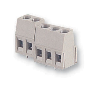
PCB terminal blocks are classified into five different categories:
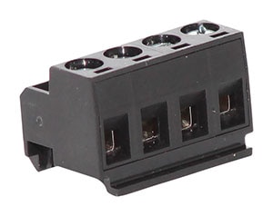
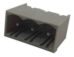
- Pluggable Terminal Block: A pluggable terminal block house multiple individual terminals, typically using screw or spring-clamp mechanisms to hold electrical contact with the conductors of the wires attached to the terminal block.
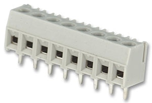
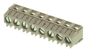
- Screw Terminal Block: Screw terminals consist of a conductive block with a threaded hole and a screw. When a wire is inserted into the threaded hole and the screw is tightened, the screw clamps down on the conductor, creating a robust and dependable electrical connection.
- Spring Terminal Block: A spring terminal block consists of a housing with individual slots or openings for wires or conductors. Inside each slot, a spring mechanism exerts pressure on the inserted conductor, creating an electrical connection without screws or soldering.
- Barrier Terminal Block: A barrier terminal block typically consists of a plastic or insulating housing with multiple terminals separated by partitions or barriers. Each terminal uses a screw or clamp mechanism for securing wires, and the barriers isolate and protect adjacent terminals from accidental contact.
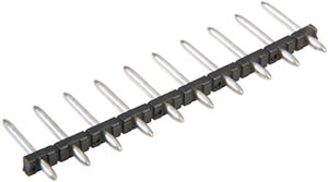
- Pin Header Connector: A pin header connector contains of a row of male pins or metal connectors, generally within a plastic housing, that can be inserted into a corresponding female socket or receptacle.
How to Connect a Wire to a Terminal Block
There are a handful of methods for securing a wire on a terminal block:
- Screw Terminal: The wire is held in place firmly against the conductor by a clamp that is closed by tightening a screw.
- Push Button Terminal Block: The wire is fastened to the conductor using a spring clamp that is released by pressing a button.
- Push-in Terminal Blocks: The wire is held securely in place using a spring or clamp mechanism, which exerts pressure automatically when a wire is inserted.
What are high-density interconnect (HDI) PCBs?
High-density interconnect (HDI) PCBs are multilayer circuit boards printed with a higher wiring density per unit area when compared to traditional printed circuit boards. They take advantage of blind, buried, and micro vias, vias in pads, and fragile traces to pack more components into a smaller area.
What PCB design files do you need to manufacture and assemble a PCB?
PCB assembly and manufacture can only start if the following design files are available:
- Gerber File: A Gerber file is a standard file format used to convey information about the design of a PCB. Gerber files are essential for the manufacturing process because they provide detailed instructions on how to create the PCB's physical layout; it includes information about the PCB's copper layers, solder mask, silk screen, and drill holes. Gerber files are created using PCB design software tools.
- Centroid File: A centroid or pick-and-place file is a circuit board's digital blueprint. It contains the position and orientation of all SMDs, including the reference designator, X and Y position, orientation of components, and component packages.
- Bill of Materials: The Bill of Materials (BOM) is a comprehensive list of all components used in the assembly of a PCB. It should include part numbers, descriptions, quantities, reference designators, and sometimes supplier information.
- Assembly Drawings: An assembly drawing shows all the components on the board in their assembled locations and their corresponding reference designators for identification. This file is created by exporting an image file of the board’s silkscreen layer.
- NC Drill File: The NC drill file shows the position, size, and number of holes in a PCB.
How to clean a PCB?
A PCB can be cleaned using the following methods:
- Brushing: A small, delicate brush, like a touch-up paint brush, can be used to remove dirt and dust without damaging the components.
- Compressed Air: Using compressed air to blow away debris can be effective but may also damage connections, so it should be used with extreme care.
- Vacuum Cleaners: There are special vacuum cleaners for PCBs, which come with nozzles made of non-conductive, anti-ESD material. Some include brushes that help lift dirt from the boards.
- Isopropyl Alcohol: A PCB can be cleaned using isopropyl alcohol (IPA), a Q-tip, a small brush, or a clean cotton cloth. A well-ventilated environment is required, as IPA can produce toxic fumes.
- Demineralized Water: Demineralized water can be used as an alternative to alcohol, but any excess moisture should be removed after cleaning.
- Ultrasonic PCB cleaning: An ultrasonic PCB cleaning machine sends high-frequency waves into a tank filled with a cleaning solution where the PCB is immersed, blasting away contaminants on the surface.
What is Design for Manufacturing (DFM)?
Design for Manufacturing (DFM) is a design approach focused on creating products and components with the specific goal of optimizing their manufacturability. The primary aim of DFM is to streamline and improve the manufacturing process by addressing potential design-related challenges, reducing production costs, enhancing product quality, and shortening time-to-market. DFM principles are applied throughout the product design phase to ensure that the final design is efficient and practical for mass production. The approach considers material selection, production processes, tolerances, production volumes, and tooling requirements.
What is Design for Testing (DFT)?
Design for testing (DFT) is an approach that focuses on optimizing a product’s testability and diagnostic capabilities during its manufacture and throughout its lifecycle. This method considers various design elements that influence testing and diagnostics. DFT can help reduce testing time, the cost of generating test vectors, and the need for extensive design iterations.
Frequency Asked Questions
In partnership with

Can a broken PCB be repaired?
Yes, a broken PCB can often be repaired, depending on the nature and extent of the damage. PCB repair is a common practice in electronics maintenance and troubleshooting, and it can save time and resources compared to replacing the entire PCB. These are some common PCB repair techniques and scenarios:
- Component Replacement: If a specific component on the PCB is damaged or malfunctioning, it can often be desoldered and replaced with a new one. This is a common repair method for individual components like resistors, capacitors, or integrated circuits.
- Soldering: Broken or cracked solder joints can be re-soldered to reestablish electrical connections. This is a common repair for loose connectors or damaged solder joints on through-hole or surface mount components.
- Trace Repair: If a trace (copper pathway) on the PCB is damaged or severed, it can be repaired by carefully soldering a wire or copper trace to bridge the gap. This is known as "wire jumper" repair.
- Solder Mask Repair: If solder mask insulation is damaged or missing, it can be reapplied or repaired to prevent short circuits.
- Via Repair: Damaged vias (plated-through holes) can sometimes be repaired by drilling a new hole and soldering a wire to bridge the connection between layers.
- Microscopic Repair: In high-precision applications, like aerospace or medical devices, microscopic repair techniques can be employed to repair extremely small or delicate components and traces.
How long does a PCB last?
The lifespan of a PCB can vary widely depending on several factors, including the quality of materials and manufacturing, environmental conditions, usage, and the specific application.
What causes a PCB to fail?
PCB failures can occur due to various reasons, including exposure to heat, dust, and moisture, accidental drops and falls, vibration and mechanical stress, and power surges.
How do you diagnose a PCB?
Diagnosing a PCB involves a systematic process of identifying and isolating issues or failures that affect the board's functionality. Steps include visual inspection, checking for loose components, and taking measurements at specific points with equipment, such as multimeters and oscilloscopes.
Can water damage a PCB?
Water can damage a printed circuit board (PCB) and its components. Water damage is a common concern in electronic devices and PCBs, and it can lead to a range of problems, including short circuits, corrosion, component damage, insulation breakdown, coating damage, and mold and mildew growth.
If a PCB breaks, can you glue it back together?
Yes, a broken PCB can be glued together using epoxy resins, however it is generally not a recommended method for repairing a damaged circuit board. While adhesive materials and epoxy resins are often used in PCB manufacturing for specific purposes, attempting to repair a broken PCB with glue is usually not a reliable or long-lasting solution.
Can you overheat a PCB when soldering?
Yes, it is possible to overheat a printed circuit board (PCB) when soldering, and doing so can lead to a range of problems and potential damage, including component damage, solder joint issues, delamination of traces of pads, and component displacement.
Is it ok to leave flux on a PCB?
Leaving flux residue on a PCB is not recommended, as it can have both short-term and long-term consequences. Flux is a chemical agent used in soldering to promote solder wetting and improve the quality of solder joints. While flux is important during the soldering process, it should be cleaned or removed after soldering to maintain the integrity and reliability of the PCB. Leaving flux residues on a PCB may cause problems like parasitic leakage, dendrite growth, electrochemical migration, and shorting.
Can a PCB be 3D printed?
Yes, although it is not typically used to directly create PCBs, 3D printing can produce both single-sided and double-sided PCBs. Some 3D printers can print conductive traces and are able to create simple PCBs used for rapid prototyping.
PCB Connectors from Wieland Electric
Wieland Electric provides a wide range of durable and reliable PCB connectors.

.jpg)
