element14 Community
element14 Community
    Register Log In
  • Site
  • Search
  • Log In Register
  • Community Hub
    Community Hub
    • What's New on element14
    • Feedback and Support
    • Benefits of Membership
    • Personal Blogs
    • Members Area
    • Achievement Levels
  • Learn
    Learn
    • Ask an Expert
    • eBooks
    • element14 presents
    • Learning Center
    • Tech Spotlight
    • STEM Academy
    • Webinars, Training and Events
    • Learning Groups
  • Technologies
    Technologies
    • 3D Printing
    • FPGA
    • Industrial Automation
    • Internet of Things
    • Power & Energy
    • Sensors
    • Technology Groups
  • Challenges & Projects
    Challenges & Projects
    • Design Challenges
    • element14 presents Projects
    • Project14
    • Arduino Projects
    • Raspberry Pi Projects
    • Project Groups
  • Products
    Products
    • Arduino
    • Avnet & Tria Boards Community
    • Dev Tools
    • Manufacturers
    • Multicomp Pro
    • Product Groups
    • Raspberry Pi
    • RoadTests & Reviews
  • About Us
  • Store
    Store
    • Visit Your Store
    • Choose another store...
      • Europe
      •  Austria (German)
      •  Belgium (Dutch, French)
      •  Bulgaria (Bulgarian)
      •  Czech Republic (Czech)
      •  Denmark (Danish)
      •  Estonia (Estonian)
      •  Finland (Finnish)
      •  France (French)
      •  Germany (German)
      •  Hungary (Hungarian)
      •  Ireland
      •  Israel
      •  Italy (Italian)
      •  Latvia (Latvian)
      •  
      •  Lithuania (Lithuanian)
      •  Netherlands (Dutch)
      •  Norway (Norwegian)
      •  Poland (Polish)
      •  Portugal (Portuguese)
      •  Romania (Romanian)
      •  Russia (Russian)
      •  Slovakia (Slovak)
      •  Slovenia (Slovenian)
      •  Spain (Spanish)
      •  Sweden (Swedish)
      •  Switzerland(German, French)
      •  Turkey (Turkish)
      •  United Kingdom
      • Asia Pacific
      •  Australia
      •  China
      •  Hong Kong
      •  India
      • Japan
      •  Korea (Korean)
      •  Malaysia
      •  New Zealand
      •  Philippines
      •  Singapore
      •  Taiwan
      •  Thailand (Thai)
      • Vietnam
      • Americas
      •  Brazil (Portuguese)
      •  Canada
      •  Mexico (Spanish)
      •  United States
      Can't find the country/region you're looking for? Visit our export site or find a local distributor.
  • Translate
  • Profile
  • Settings
Experts, Learning and Guidance
  • Technologies
  • More
Experts, Learning and Guidance
Ask an Expert Forum Differential amplifier problem
  • Blog
  • Forum
  • Documents
  • Leaderboard
  • Files
  • Members
  • Mentions
  • Sub-Groups
  • Tags
  • More
  • Cancel
  • New
Join Experts, Learning and Guidance to participate - click to join for free!
Actions
  • Share
  • More
  • Cancel
Forum Thread Details
  • State Verified Answer
  • Replies 38 replies
  • Answers 15 answers
  • Subscribers 301 subscribers
  • Views 9838 views
  • Users 0 members are here
Related
See a helpful answer?

Be sure to click 'more' and select 'suggest as answer'!

If you're the thread creator, be sure to click 'more' then 'Verify as Answer'!

Differential amplifier problem

Andrew J
Andrew J over 5 years ago

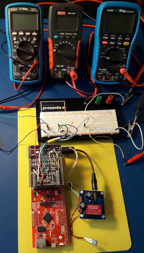
I'm working with a DAC and experimenting with removing the zero scale error - the actual output at a zero input code.  I'm on a breadboard so it isn't particularly accurate but the ZSE is 5mV to 11mV.


I set up a differential amplifier as follows - image is copied from a website, but I've confirmed and re-confirmed that my setup matches:

image

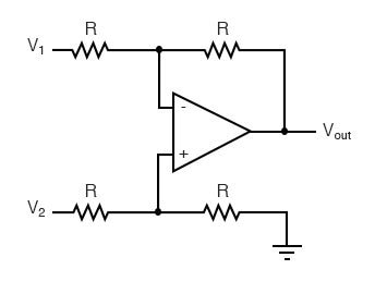
So, I have the following inputs:

V1 = 0.005mV

V2 = DACoutput

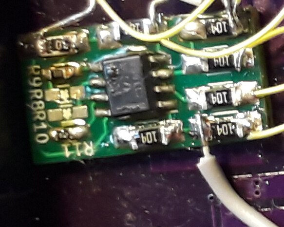
R = 100K.  All of them.

Opamp is an LM741 which is all I have on-hand, V+ = 5V, V- = ground .  It has a max offset voltage of 6mV.


Given that, I would expect Vout = V2 - V1.  Vout is connected to a 1K resistor to ground.


So the reality is that the R values are not perfectly 100K but are within the 10% spec.  Thus I wouldn't expect Vout to be an exact difference, but 'more-or-less'.


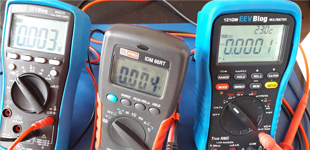
This is what I'm measuring:

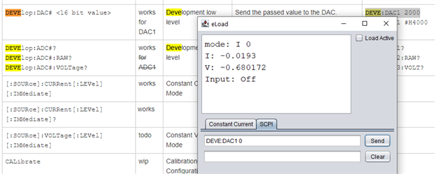
DACout (V2) = 4.06V, Vout = 4.04V

DACout (V2) = 0.011V, Vout = 3.6V


I've tried working out why with a low DACout I'm still getting a large Vout.  Measuring the resistors and plugging them into the gain formula:


Vout = -0.005 * (99.03/99.5) + 0.011 * (99.21/(99.05+99.21)) * ((99.5+99.03)/99.5)

Vout = (-0.005 * 0.995) + (0.011 * 0.500 * 1.995)

Vout = -0.005 + 0.011 = 0.006


So, essentially, my calculation confirms what I would expect the amplifier to do with a -0.005mV and 0.011mV input.


I can't figure out where I've gone wrong, can anyone give me some pointers?

Attachments:
2477.LM741.asc.zip
  • Sign in to reply
  • Cancel

Top Replies

  • michaelkellett
    michaelkellett over 5 years ago +5 verified
    What power do you have connected to the 741 - it's not rail to rail capable it needs positive and negative supplies, +/- 10V is the minimum recommended. The input common mode range is +/- 12V when running…
  • michaelkellett
    michaelkellett over 5 years ago in reply to Andrew J +5 suggested
    If you want to sink any current at 0V you need a negative supply. You could consider using +/- 5V supplies (+/- 10 if you stick with the 741 ) You can do a lot of this without spending money by using a…
  • Jan Cumps
    Jan Cumps over 5 years ago in reply to Andrew J +4 suggested
    Yes, we're doing it the naive way. That's why I hope that analog / DAC experts chime in and show the shining path to real world solutions. In the eLoad we made, things like OpAmp offset, quiescent current…
Parents
  • Jan Cumps
    0 Jan Cumps over 5 years ago

    I'm preparing my board for some measurement.

    Soldered in a measurement wire at the subtractor output:

    image


    A DMM on DAC A - the one that I use to set the dc load point

    One on DAC B, - the one I use to offset A's DC offset

    One on that output of the opamp wire I just soldered in ...

    setimage


    I can now use the GUI to talk to the individual DACs. I created SCPI commands for that in the firmware:

    image


    ... and then measure the effect ...

    • Cancel
    • Vote Up 0 Vote Down
    • Sign in to reply
    • Verify Answer
    • Cancel
  • Jan Cumps
    0 Jan Cumps over 5 years ago in reply to Jan Cumps

    So it's actually working:


    image

    the photo shows the meters in volt range. The measurements below are done with all in mV range.


    Initially, I get about 2 mV out off the subtractor


    I've set the DAC1 to 200. That's the region where mine is in the linear part. Under that, it doesn't move below the offset.

    • DEVE:DAC1 200


    DAC 1 outputs 4.92 mV

    DAC 2 1.64 mV

    OpAmp is still at 2 mV


    At this point, any change in DAC1 increases the output.

    This is the range I want to work from - starting DAC1 from 200 - and consider that 0.

    So I have to work away the 2 mV offset with DAC 2.


    Starting with value 10:

    • DEVE:DAC2 10


    DAC2 is now 2.04 mV

    OpAmp is at 1.55 mV


    • DEVE:DAC2 20


    DAC2 is now 2.42 mV

    OpAmp 1.19 mV


    • DEVE:DAC2 30


    DAC2 is now 2.85 mV

    OpAmp 0.75 mV


    • DEVE:DAC2 40


    DAC2 is now 3.24 mV

    OpAmp 0.35 mV


    • DEVE:DAC2 45


    DAC2 is now 3.46 mV

    OpAmp 0.13 mV


    • DEVE:DAC2 50


    DAC2 is now 3.65 mV

    OpAmp -0.06 mV <- overcompensated


    The following two are the closest I can get to 0...


    • DEVE:DAC2 48


    DAC2 is now 3.56 mV

    OpAmp 0.02 mV


    • DEVE:DAC2 49


    DAC2 is now 3.62 mV

    OpAmp -0.02 mV


    image


    In theory, I could automate this by connecting the last uncommitted ADC I have on the board to the output of the subtractor and let the system run through the paces itself until it settles for the lowest linear point, then 0 it out ...

    • Cancel
    • Vote Up +1 Vote Down
    • Sign in to reply
    • Verify Answer
    • Reject Answer
    • Cancel
  • Andrew J
    0 Andrew J over 5 years ago in reply to Jan Cumps

    Is that last 20uV the INL and DNL error possibly?  I'd say it was a good result.  I presume you're also losing 3.56mV off the FSR?  Will that have any impact?  It would be useful to stretch the output to a genuine 0mV and full scale range V but I suspect you may lose some output accuracy at various points in that range.


    As I was experimenting with the OpAmp to do this with a voltage divider I was able to link in my head what I was trying to achieve with what you were doing with the DAC offset compensation board you created (I'd read that a while ago.)  As I've thought about it more over the last day and a bit, I think your approach is likely to be the more accurate as the resistor/potentiometer is unlikely to be as good in terms of drift AND I can't automatically determine and adjust compensation. 


    I'd further thought that I could use an ADC input to change the compensating DAC output so that it stayed as accurate as possible - I think that's what you are eluding to in your last sentence.  I was intending to set the software up to run automatic compensation for offset and gain errors across all DAC outputs so that as, say, temperatures rose, it could try and maintain some accuracy.  This would just be an additional step to make sure that it could output close to 0mV as possible.  This could be done at regular intervals, say when output was turned off and nothing was being driven.


    I can't see having an extra DAC on the board any more expensive in terms of cost or real estate than a set of voltage dividers and because I'm thinking of starting in a more accurate place I will have a spare DAC, and maybe ADC.

    • Cancel
    • Vote Up 0 Vote Down
    • Sign in to reply
    • Verify Answer
    • Cancel
  • Jan Cumps
    0 Jan Cumps over 5 years ago in reply to Andrew J
    Is that last 20uV the INL and DNL error possibly?  I'd say it was a good result.

    The offset of DAC 1 is higher than that. But because DAC 2 also has offset by itself, it has already handled part of the work by just plugging it into the opamp.


    I presume you're also losing 3.56mV off the FSR?  Will that have any impact?


    Yes I'm loosing range. No it's not impacting because I have enough range over to drive the circuit and FET as required (there's headroom at the high end - also a waste of resolution of course. Playing with the circuit's gain can tune this to maximum viable).


    I don't know if I made that clear but, although this fixes the offset of DAC 1, it doesn't fix another issue I have in the eLoad, where it behaves bad at the 0 range.

    But that's not a DAC issue. That has to do with the analog control circuit.

    I haven't found the reason for that yet...


    As I was experimenting with the OpAmp to do this with a voltage divider I was able to link in my head what I was trying to achieve with what you were doing with the DAC offset compensation board you created (I'd read that a while ago.)  As I've thought about it more over the last day and a bit, I think your approach is likely to be the more accurate as the resistor/potentiometer is unlikely to be as good in terms of drift AND I can't automatically determine and adjust compensation.


    I think it will - except if you use a 10-turn trimmer. It was not the reason for my approach though.

    I wanted to introduce a programmable compensation instead of manual trimmers. More for my own learning than for practical purpose ...


    I'd further thought that I could use an ADC input to change the compensating DAC output so that it stayed as accurate as possible - I think that's what you are eluding to in your last sentence


    Yes. And I have the hardware to do that. Just have to bodge yet another wire in - but that's prototyping.

    I've currently disabled the last free ADC in the firmware because it's unconnected, and sampling takes time. But with the last improvement I did in the ADC process, I have enough resources to do that.

    I'd just need the burning desire to get on with it image...


    I can't see having an extra DAC on the board any more expensive in terms of cost or real estate than a set of voltage dividers and because I'm thinking of starting in a more accurate place I will have a spare DAC, and maybe ADC.

    Robert Peter Oakes and I decided to go for 4 channel DAC and ADC. While we only needed one DAC and 3 (initial 2, before we introduced temperature protection) ADCs.

    Because this isn't a commercial product, and we wanted to play with those ICs (they are expensive - but those are the decisions you make when it's educational), we didn't have to worry about that a lot.

    In the end it turned out to be a good thing for this design, because it allows for additional experimentation.


    There's also a i2c bus extender there. 8 pins of which only one is used for enabling the load on command.

    The 7 others are free and could be used for GPIO, fan control, ... . The firmware would have to be altered, but this would not be intrusive...

    image

    They are on the isolated side of the circuit so safe to use. I didn't put breakout pads but you can remove their associated resistor (needed when not in use to ease the expander) and use the resistor pad to get at the I/O.

    Not 100% hack friendly, but it gets you a long way ...

    • Cancel
    • Vote Up +1 Vote Down
    • Sign in to reply
    • Verify Answer
    • Cancel
  • Andrew J
    0 Andrew J over 5 years ago in reply to Jan Cumps

    Nice one.  I'm busy pulling together a more 'final' schematic to turn into a PCB for more work - I'm going to go the same route as yourself for compensating rather than the divider route: I really want to have programmable compensation.  It'll be interesting as there will be offset, gain, INL and DNL errors on all DACs and ADCs so there is some compounding going on as well!  I have 2 spare digital outputs on my isolator available if I need them, which I suspect I will right now. 


    The post you made here ought to get x-refd from your main blog as it's very useful.

    • Cancel
    • Vote Up 0 Vote Down
    • Sign in to reply
    • Verify Answer
    • Cancel
Reply
  • Andrew J
    0 Andrew J over 5 years ago in reply to Jan Cumps

    Nice one.  I'm busy pulling together a more 'final' schematic to turn into a PCB for more work - I'm going to go the same route as yourself for compensating rather than the divider route: I really want to have programmable compensation.  It'll be interesting as there will be offset, gain, INL and DNL errors on all DACs and ADCs so there is some compounding going on as well!  I have 2 spare digital outputs on my isolator available if I need them, which I suspect I will right now. 


    The post you made here ought to get x-refd from your main blog as it's very useful.

    • Cancel
    • Vote Up 0 Vote Down
    • Sign in to reply
    • Verify Answer
    • Cancel
Children
  • michaelkellett
    0 michaelkellett over 5 years ago in reply to Andrew J

    If I understand correctly what you are trying to do it might be a lot simpler and cheaper to use a singe DAC with 2 more bits and a deliberate fixed offset on the output and do the compensation entirely in software.

    You could still make it fully automatic by adding an ADC but this needs to be good compared with the DAC.

    Don't forget the voltage reference - it's quite tricky to get even 12 bit accuracy over  a modest temperature range.


    MK

    • Cancel
    • Vote Up +2 Vote Down
    • Sign in to reply
    • Verify Answer
    • Reject Answer
    • Cancel
  • Andrew J
    0 Andrew J over 5 years ago in reply to michaelkellett

    Thanks Michael,


    I’ve pretty much decided to go the same way as Jan did as I now have a spare ADC and DAC on hand.  I also have a REF5040 on hand which I’m currently using with those two components - the new ADC and DACs I’m thinking about have internal references which have better stats than the REF5040, at first check but I need to reconfirm as part of final checking.  I just need to gird my loins for soldering a DFN package!

    • Cancel
    • Vote Up +1 Vote Down
    • Sign in to reply
    • Verify Answer
    • Cancel
element14 Community

element14 is the first online community specifically for engineers. Connect with your peers and get expert answers to your questions.

  • Members
  • Learn
  • Technologies
  • Challenges & Projects
  • Products
  • Store
  • About Us
  • Feedback & Support
  • FAQs
  • Terms of Use
  • Privacy Policy
  • Legal and Copyright Notices
  • Sitemap
  • Cookies

An Avnet Company © 2025 Premier Farnell Limited. All Rights Reserved.

Premier Farnell Ltd, registered in England and Wales (no 00876412), registered office: Farnell House, Forge Lane, Leeds LS12 2NE.

ICP 备案号 10220084.

Follow element14

  • X
  • Facebook
  • linkedin
  • YouTube