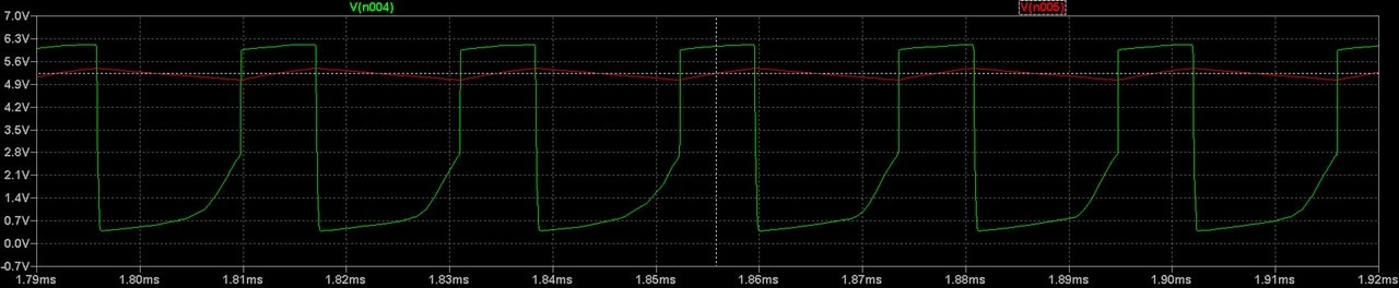
Hi,I am a beginner in electronics and i just wanted to help with a certain circuit of mine that I was handling and it was a boost converter but the input 3.7v is the same as the output and wanted the output to be 5v DC
Attachments:
 | |
 |
Be sure to click 'more' and select 'suggest as answer'!
If you're the thread creator, be sure to click 'more' then 'Verify as Answer'!
Hi,I am a beginner in electronics and i just wanted to help with a certain circuit of mine that I was handling and it was a boost converter but the input 3.7v is the same as the output and wanted the output to be 5v DC
| |
|