Hi, I am stuck with my little project here and looking for help. The situation
I have successfully created a block design which uses the axiDMA IP and loops it through a FIFO back to the SW. This is required by an example program in Vitis I am using as a foundation to use the DMA, with my setup I got the example to execute succesfully.
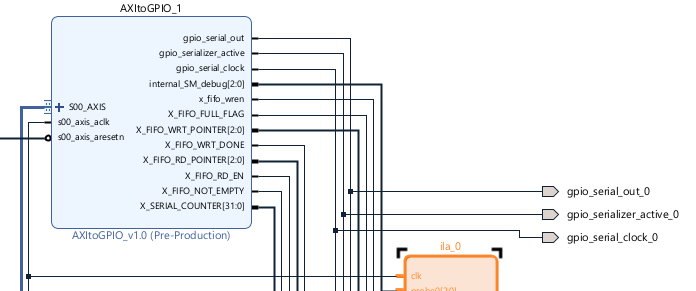
Now where I ran into issues: I have created ant tested a custom IP which serializes these 32b values from AXI to a pin which I want to route to an external pin. The IP works which I validated through a testbench and even on the MPSoC using an ILA, but I cant see any reaction on the pin.
I have reviewed the implemented design and the net is properly generated (design connected to output buffer and output buffer connected to external pin).
Am I missing something, which parts of the flow could cause errors like this? Is there maybe some configuration required through Vitis?
Some of my resources:
Constraint:
set_property PACKAGE_PIN F3 [get_ports x_gpio_serial_clock_0]
set_property PACKAGE_PIN F2 [get_ports x_gpio_serial_out_0]
set_property PACKAGE_PIN N2 [get_ports x_gpio_serializer_active_0]
set_property IOSTANDARD LVCMOS18 [get_ports x_gpio_serializer_active_0]
set_property IOSTANDARD LVCMOS18 [get_ports x_gpio_serial_out_0]
set_property IOSTANDARD LVCMOS18 [get_ports x_gpio_serial_clock_0]
Top level instantiation:
entity design_1_wrapper is
port (
x_gpio_serial_clock_0 : out STD_LOGIC;
x_gpio_serial_out_0 : out STD_LOGIC;
x_gpio_serializer_active_0 : out STD_LOGIC
);
end design_1_wrapper;
architecture STRUCTURE of design_1_wrapper is
component design_1 is
port (
gpio_serial_out_0 : out STD_LOGIC;
gpio_serializer_active_0 : out STD_LOGIC;
gpio_serial_clock_0 : out STD_LOGIC
);
end component design_1;
begin
design_1_i: component design_1
port map (
gpio_serial_clock_0 => x_gpio_serial_clock_0,
gpio_serial_out_0 => x_gpio_serial_out_0,
gpio_serializer_active_0 => x_gpio_serializer_active_0
);
end STRUCTURE;
My custom Serializer in the block design: