


It sounds great to make an online PCB Design and share with all the people and also you could edit Online PCB .
Do you think it is great ? There are some online Circuit Designer ,for example , circuitlab , upverter
and easyeda .
For there are no PCB layout function on Circuit Lab ,and I need to register an account on Upverter so I could start to design , so I choose to experience EasyEDA.
And certainly registering an account will provides us much more functions , that will help you a lot in designing circuits ,saving your projects on the cloud sever and sharing with friends or colleagues.Let us look at the Register and Login interface first .
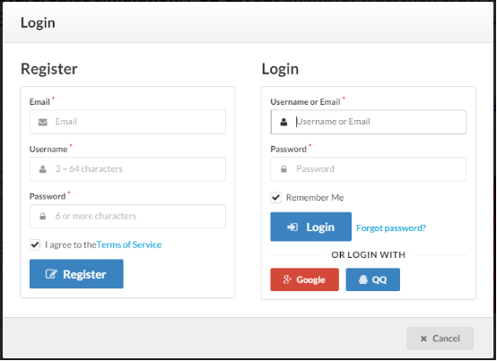
——The Register and Login Interface .
Then create a new Project:
Check what are there on the website main page .

——The mainpage of https://easyeda.com/
Click New Project and we can go to the Editor :https://easyeda.com/editor
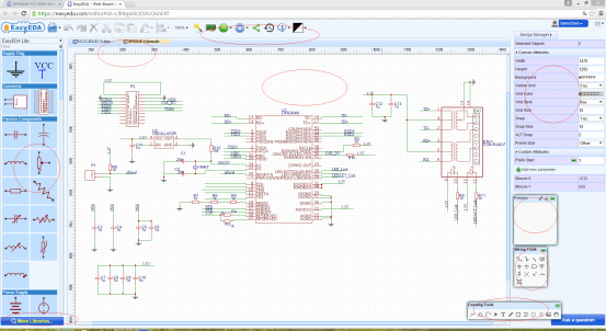
——The diagram of the Editor
On the Editor Interface, there are Toolbar, Schematic,Design Manager, Wiring Tools ,Drawing Tools,Preview. And on the left size there are items like My Projects, My Parts, Shared with me,Favorite Parts, EasyEDA Libs &General Package.
Let me introduce How to draw a schematic now .
For example , draw a LED Light Circuit. You could choose the component on the left-hand side :Using easyeda Libs ,click to put a resistor , a led Light , a power source ,a ground ,a capacitor . Then connect them into a circuit with wire in wiring Tools.The color of the Schematic background , the color of the wire or the text , or the Netlist ICON and so forth can be changed in colors. OK ,let us See the completed schematic .
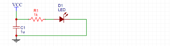
——A Led Light Schematic Example .
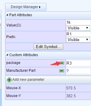
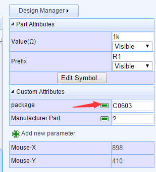
Then choose package for every component , the resistor 0603 package, the LED 3MM,the capacitor choose 0805 package.
Click the component ,then go to the design Manager, then click the space in the package , then it will come out with the dialog of “Update the symbols’ Package”Then choose the package in the user package ,favorite Package ,or general Package .Or input the package name in the space if you know package name in your parts your favorite parts or in the system package .
You could also preview the package of the components. For instance , choosing an 0805 package for a capacitor .
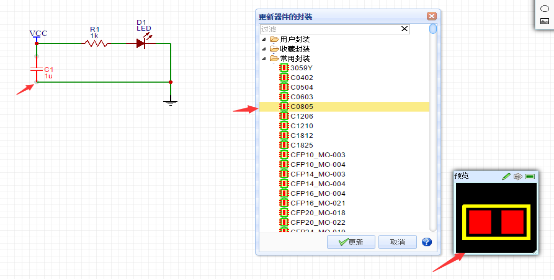
——Choose the Package for the component and preview.
Then you could easily know whether the component is suitable for your design.
You could also drag the update component package and preview Tool to proper position as you expect.
Then convert the schematic to PCB .
About How to convert Schematic to PCB , Please refer to File “How to convert Schematic to PCB”.
For most of the simple circuits , you could choose auto route to layout the PCB .Thanks to hardworking of EasyEDA team ,the EasyEDA could do online PCB auto routing .It feels wonderful and convenient to route simple one-or-two layer boards .
Check the effect of auto routing .
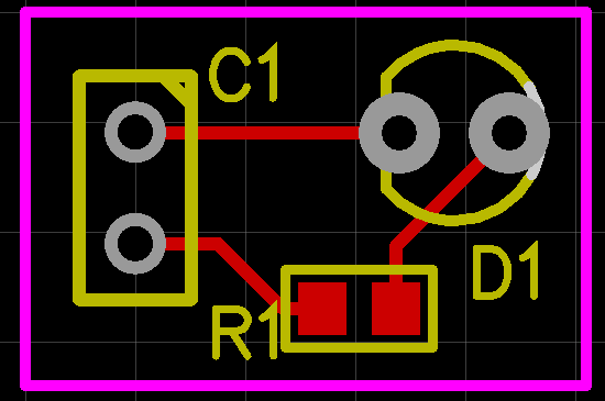
——The effect of Auto Routing1
It seems so simple that I could not be brave enough to put it in online ,but it is just used to illustrate what it is like when auto routing very simple circuits.
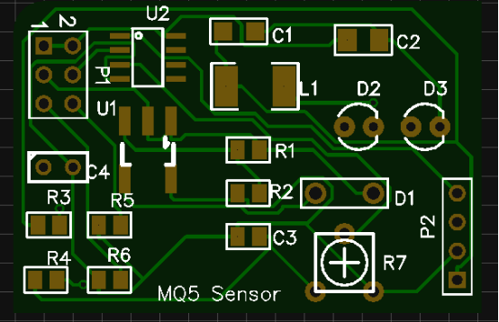
Let me show another complex auto routing effect diagram:https://easyeda.com/GerryChen/MQ5_Sensor_Module_Project-F1VdvpGYg
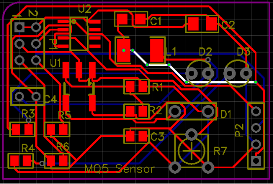
——The Effect of Auto Routing2.
——The Effect of Photo Preview
Then you could have a photo preview to check whether the Layout can be used in real Product .
For More complex Project , you could also choose auto routing . You could just slightly adjust the Routing .
Even though it could auto route, I think for most of complex projects ,we should route the PCB manually .
In summary , I feel it provides us with much convenience to build small-scale or middle-scale projects anywhere accessible to Internet . I need not to install an EDA software on my PC ,neither do I need to create most of the Schematic Lib or PCB Lib personally .I need not to just use the Design of myself , I could also apply some online electronic designs from electronic freaks or engineers , no matter you are beginners or professional engineers , I could learn knowledge from your design, I can get inspiration from your simple designs or complex designs, from your industrialized designs or just the designs out of your hobbies . Sometimes, if I want to create a Project ,I could use most of the Sample Designs ,most of the Online Schematic Lib or PCB Lib. If there is not Lib I wanted , I could build one online and it could be shared with all the Online Designers. I feel it is not just saving most of my time on Design, but also provides convenience to all the online Designers .There are fulfillment when I finish many SCH Lib or PCB Lib or One Complete Project and they would possibly be adopted.