element14 Community
element14 Community
    Register Log In
  • Site
  • Search
  • Log In Register
  • About Us
  • Community Hub
    Community Hub
    • What's New on element14
    • Feedback and Support
    • Benefits of Membership
    • Personal Blogs
    • Members Area
    • Achievement Levels
  • Learn
    Learn
    • Ask an Expert
    • eBooks
    • element14 presents
    • Learning Center
    • Tech Spotlight
    • STEM Academy
    • Webinars, Training and Events
    • Learning Groups
  • Technologies
    Technologies
    • 3D Printing
    • FPGA
    • Industrial Automation
    • Internet of Things
    • Power & Energy
    • Sensors
    • Technology Groups
  • Challenges & Projects
    Challenges & Projects
    • Design Challenges
    • element14 presents Projects
    • Project14
    • Arduino Projects
    • Raspberry Pi Projects
    • Project Groups
  • Products
    Products
    • Arduino
    • Avnet Boards Community
    • Dev Tools
    • Manufacturers
    • Multicomp Pro
    • Product Groups
    • Raspberry Pi
    • RoadTests & Reviews
  • Store
    Store
    • Visit Your Store
    • Choose another store...
      • Europe
      •  Austria (German)
      •  Belgium (Dutch, French)
      •  Bulgaria (Bulgarian)
      •  Czech Republic (Czech)
      •  Denmark (Danish)
      •  Estonia (Estonian)
      •  Finland (Finnish)
      •  France (French)
      •  Germany (German)
      •  Hungary (Hungarian)
      •  Ireland
      •  Israel
      •  Italy (Italian)
      •  Latvia (Latvian)
      •  
      •  Lithuania (Lithuanian)
      •  Netherlands (Dutch)
      •  Norway (Norwegian)
      •  Poland (Polish)
      •  Portugal (Portuguese)
      •  Romania (Romanian)
      •  Russia (Russian)
      •  Slovakia (Slovak)
      •  Slovenia (Slovenian)
      •  Spain (Spanish)
      •  Sweden (Swedish)
      •  Switzerland(German, French)
      •  Turkey (Turkish)
      •  United Kingdom
      • Asia Pacific
      •  Australia
      •  China
      •  Hong Kong
      •  India
      •  Korea (Korean)
      •  Malaysia
      •  New Zealand
      •  Philippines
      •  Singapore
      •  Taiwan
      •  Thailand (Thai)
      • Americas
      •  Brazil (Portuguese)
      •  Canada
      •  Mexico (Spanish)
      •  United States
      Can't find the country/region you're looking for? Visit our export site or find a local distributor.
  • Translate
  • Profile
  • Settings
Power & Energy
  • Technologies
  • More
Power & Energy
Forum Help needed for a USB-C Power Delivery Circuit
  • Blog
  • Forum
  • Quiz
  • Documents
  • Polls
  • Events
  • Mentions
  • Sub-Groups
  • Tags
  • More
  • Cancel
  • New
Actions
  • Share
  • More
  • Cancel
Forum Thread Details
  • Replies 21 replies
  • Subscribers 286 subscribers
  • Views 7598 views
  • Users 0 members are here
  • usb-c
  • mp5031
  • usb-c power delivery
Related

Help needed for a USB-C Power Delivery Circuit

shabaz
shabaz over 2 years ago

Table of Contents

  • The Problem:
  • The Circuit
  • Programming and Verifying the Chip
  • My Configuration Notes

Hi,

I'm having trouble bringing up a circuit and I figured I'd ask here in case anyone can spot where I'm going wrong. I will also raise it with the chip manufacturer and point them to this discussion so that they can see the detail more easily. Unfortunately, there seems to be almost zero information on the Internet about this chip, beyond the datasheet, so I have nothing to compare against.

The Problem:

A USB-C circuit consisting of a DC-DC converter and a USB-C Power Delivery controller isn't functioning as expected. According to the PDF datasheet of the MP5031 USB-C Power Delivery controller chip, the chip has a default configuration, but I need to program via I2C certain register settings so that it functions with the MP2491C DC-DC converter chip I have selected. The I2C registers are supposed to be one-time-programmable (OTP), so if I program them incorrectly, the chip needs to be desoldered and replaced with a new one. I don't mind doing that, but only if I definitely have messed that up.

The specific IC I am using is part code MP5031GRE-00A3-P.

I have programmed the I2C register settings in the manner that I thought was correct. After programming, I read the settings and verified that they were what I expected. 

All good so far. However, after I reboot, and re-read the I2C registers, the settings are back to the defaults!

There is this snippet in the datasheet:

"These registers are one-time programmable (OTP). If the MP5031’s VCC voltage (VCC) exceeds the UVLO rising threshold, then the OTP items are loaded to the I2C register."

I have (of course) checked the VCC voltage, and it is 5.01V which is what it should be. So, now I'm unsure what to do : ) I don't want to attempt to re-program the OTP registers, in case that messes things up. Besides, I'm pretty confident they were programmed because, as mentioned, I read the registers after programming. 
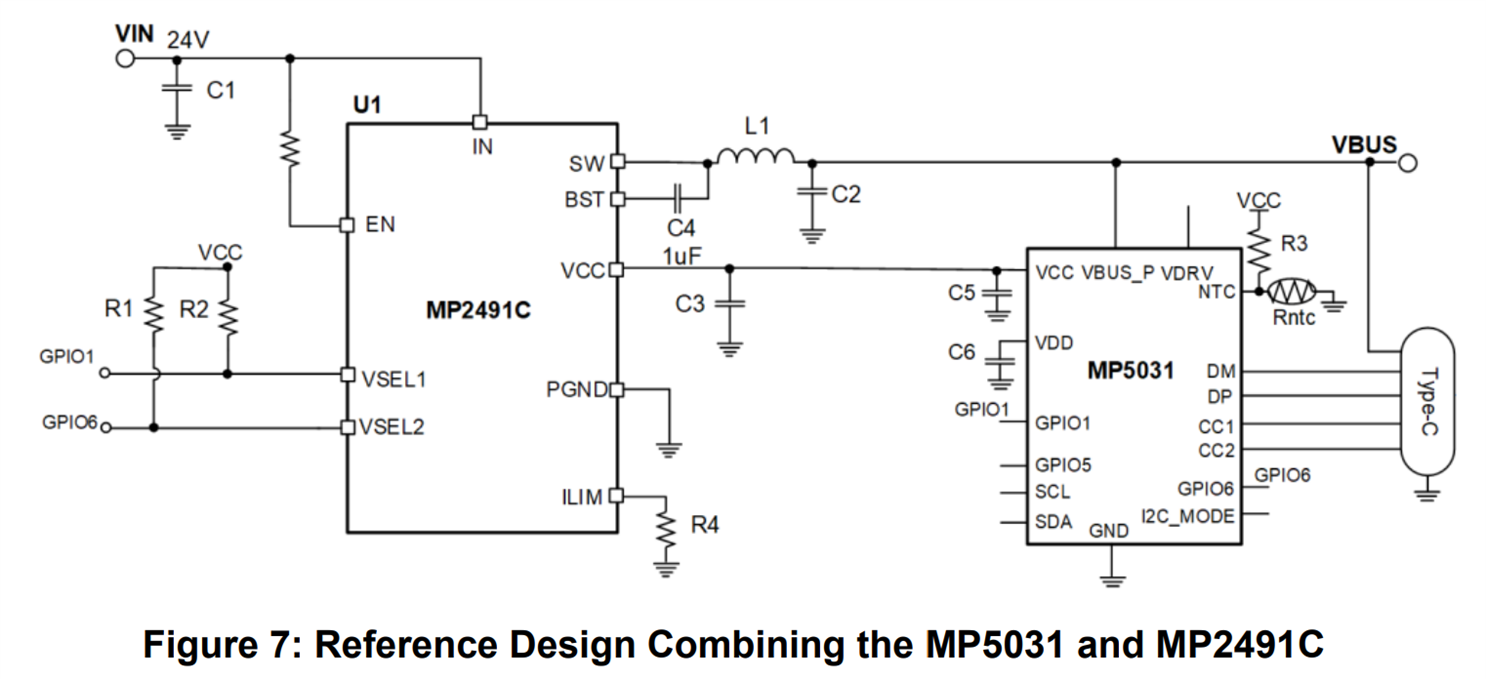
The Circuit

My circuit was based on this diagram:

image

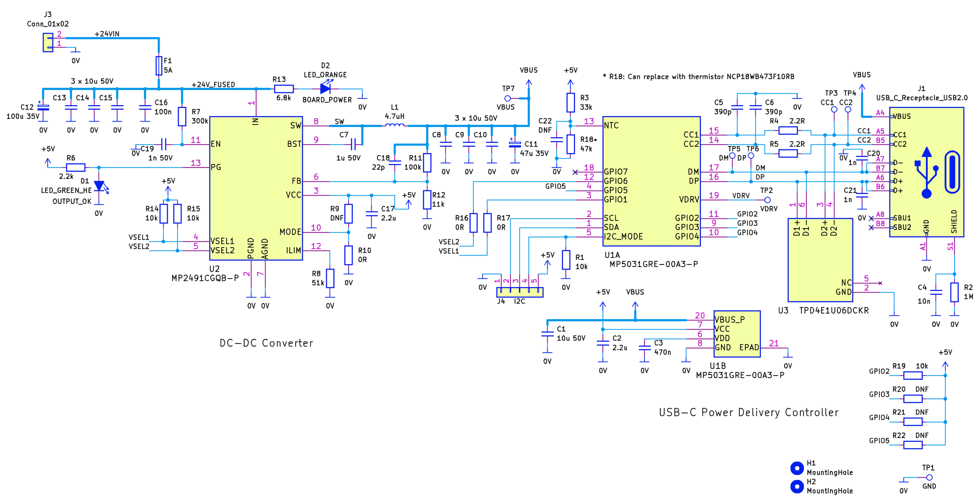
My actual implementation was this (click the diagram to enlarge it):

image

Programming and Verifying the Chip

To perform the configuration, I used the connector J4 in the circuit, snippet:

image

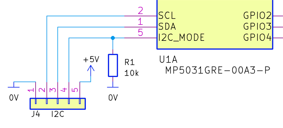
I shorted pins 4 and 5 of the connector (so that I2C_MODE was high which enables the I2C slave), then powered up the board, and then performed the I2C operations using a microcontroller.

The registers inside the chip are all 16-bit wide, and the register addresses are 0x00 to 0x14, with 0x13 missing (it is undocumented, so I didn't read or write that address).

This was the default configuration within the chip (before I wrote my updates):

(note that for each 16-bit register value, the low byte comes first, followed by the high byte, so that (say) "Hex Data F8 02" refers to a register containing the 16-bit value of 0x02F8; this is in accordance with what the datasheet mentions about the order of the bytes over I2C).

Reading chip contents
Reading: Reg: 0x00
         Hex Data: F8 02
Reading: Reg: 0x01
         Hex Data: 64 00
Reading: Reg: 0x02
         Hex Data: 2C 0D
Reading: Reg: 0x03
         Hex Data: B4 00
Reading: Reg: 0x04
         Hex Data: 2C 01
Reading: Reg: 0x05
         Hex Data: 2C 01
Reading: Reg: 0x06
         Hex Data: 2C 01
Reading: Reg: 0x07
         Hex Data: 90 01
Reading: Reg: 0x08
         Hex Data: 2C 01
Reading: Reg: 0x09
         Hex Data: 21 D2
Reading: Reg: 0x0A
         Hex Data: 3C 00
Reading: Reg: 0x0B
         Hex Data: 81 00
Reading: Reg: 0x0C
         Hex Data: 0A 0A
Reading: Reg: 0x0D
         Hex Data: 31 90
Reading: Reg: 0x0E
         Hex Data: F0 98
Reading: Reg: 0x0F
         Hex Data: 3C 3C
Reading: Reg: 0x10
         Hex Data: 00 00
Reading: Reg: 0x11
         Hex Data: 03 00
Reading: Reg: 0x12
         Hex Data: 00 80
Reading: Reg: 0x14
         Hex Data: 00 00

These were the configuration changes I made, there were just three registers I changed:

*** Programming chip ***
#1: Changing register 0x0B from hex 81 00 to 85 00
Writing: Reg: 0x0B
         Hex Data: 85 00
#2: Changing register 0x0D from hex 31 90 to 34 90
Writing: Reg: 0x0D
         Hex Data: 34 90
#3: Changing register 0x0E from hex F0 98 to C8 98
Writing: Reg: 0x0E
         Hex Data: C8 98
*** Programming complete, 3 registers updated ***

After that, I read every register, to ensure each value was expected:

Reading: Reg: 0x00
         Hex Data: F8 02
Register 0x00 contains expected value
Reading: Reg: 0x01
         Hex Data: 64 00
Register 0x01 contains expected value
Reading: Reg: 0x02
         Hex Data: 2C 0D
Register 0x02 contains expected value
Reading: Reg: 0x03
         Hex Data: B4 00
Register 0x03 contains expected value
Reading: Reg: 0x04
         Hex Data: 2C 01
Register 0x04 contains expected value
Reading: Reg: 0x05
         Hex Data: 2C 01
Register 0x05 contains expected value
Reading: Reg: 0x06
         Hex Data: 2C 01
Register 0x06 contains expected value
Reading: Reg: 0x07
         Hex Data: 90 01
Register 0x07 contains expected value
Reading: Reg: 0x08
         Hex Data: 2C 01
Register 0x08 contains expected value
Reading: Reg: 0x09
         Hex Data: 21 D2
Register 0x09 contains expected value
Reading: Reg: 0x0A
         Hex Data: 3C 00
Register 0x0A contains expected value
Reading: Reg: 0x0B
         Hex Data: 85 00
Register 0x0B expected hex 81 00 but chip contains 85 00
Register 0x0B has been programmed with expected update
Reading: Reg: 0x0C
         Hex Data: 0A 0A
Register 0x0C contains expected value
Reading: Reg: 0x0D
         Hex Data: 34 90
Register 0x0D expected hex 31 90 but chip contains 34 90
Register 0x0D has been programmed with expected update
Reading: Reg: 0x0E
         Hex Data: C8 98
Register 0x0E expected hex F0 98 but chip contains C8 98
Register 0x0E has been programmed with expected update
Reading: Reg: 0x0F
         Hex Data: 3C 3C
Register 0x0F contains expected value
Reading: Reg: 0x10
         Hex Data: 00 00
Register 0x10 contains expected value
Reading: Reg: 0x11
         Hex Data: 03 00
Register 0x11 contains expected value
Reading: Reg: 0x12
         Hex Data: 00 80
Register 0x12 contains expected value
Reading: Reg: 0x14
         Hex Data: 00 00
Register 0x14 contains expected value
Chip contents do not match reference blank chip, but match the expected updates.
The chip was successfully programmed previously.
                                                                                

But, after power-cycling the board, this is the result:

Examining chip contents against blank reference chip
Reading: Reg: 0x00
         Hex Data: F8 02
Register 0x00 contains expected value
Reading: Reg: 0x01
         Hex Data: 64 00
Register 0x01 contains expected value
Reading: Reg: 0x02
         Hex Data: 2C 0D
Register 0x02 contains expected value
Reading: Reg: 0x03
         Hex Data: B4 00
Register 0x03 contains expected value
Reading: Reg: 0x04
         Hex Data: 2C 01
Register 0x04 contains expected value
Reading: Reg: 0x05
         Hex Data: 2C 01
Register 0x05 contains expected value
Reading: Reg: 0x06
         Hex Data: 2C 01
Register 0x06 contains expected value
Reading: Reg: 0x07
         Hex Data: 90 01
Register 0x07 contains expected value
Reading: Reg: 0x08
         Hex Data: 2C 01
Register 0x08 contains expected value
Reading: Reg: 0x09
         Hex Data: 21 D2
Register 0x09 contains expected value
Reading: Reg: 0x0A
         Hex Data: 3C 00
Register 0x0A contains expected value
Reading: Reg: 0x0B
         Hex Data: 81 00
Register 0x0B contains expected value
Reading: Reg: 0x0C
         Hex Data: 0A 0A
Register 0x0C contains expected value
Reading: Reg: 0x0D
         Hex Data: 31 90
Register 0x0D contains expected value
Reading: Reg: 0x0E
         Hex Data: F0 98
Register 0x0E contains expected value
Reading: Reg: 0x0F
         Hex Data: 3C 3C
Register 0x0F contains expected value
Reading: Reg: 0x10
         Hex Data: 00 00
Register 0x10 contains expected value
Reading: Reg: 0x11
         Hex Data: 03 00
Register 0x11 contains expected value
Reading: Reg: 0x12
         Hex Data: 00 80
Register 0x12 contains expected value
Reading: Reg: 0x14
         Hex Data: 00 00
Register 0x14 contains expected value
Chip contents match reference blank chip, i.e. chip appears to be unprogrammed

My Configuration Notes

Here is my reasoning for why I modified the register values that I did.

RegAddr RegName Notes Change
0x00 PDO_TYPE Default is OK (all power data objects are enabled).
Can read this, to see the software revision. Read 15..0 bits, and bits 15..10 contain the software revision.
D0..7 = f8, D8..15 = 02
0x01 PDO_V1 Read only. Should return 5V which is 0x064 (only bits 9..0 are relevant). 0x64 x 50mV = 5000mV = 5V
0x02 PDO_I1 Default should be fine, which is 3A (only bits 9..0). 3A/0.01A = 300 which Is 0x12C
0x03 PDO_V2 Default is 9V
0x04 PDO_I2 Default is 3A
0x05 PDO_V3 Default is 15V
0x06 PDO_I3 Default is 3A
0x07 PDO_V4 Default is 20V
0x08 PDO_I4 Default is 3A
0x09 PDO_V5 What is the default? Anyway I left this unchanged.
0x0A PDO_I5 What is the default? I left this unchanged.
0x0B CTL1 Bits 2..0 by default are 0x01 (i.e. 001 binary), but this needs changing! Those three bits need to change to 0x05 (i.e. 101 binary). This sets the chip to be able to select PDO2,3 or 4 by using the PDO2_SEL and PDO3_SEL pins. Set to hex 85 00
0x0C CTL2 Can write a 1 to the the most significant bit (bit 15) to perform a hard reset. I left this register alone, because I don’t understand some of it. I think the defaults are OK.
0x0D CTL3 Bits 2..0 are by default 001 binary (0x01) but need to be changed to 100 binary (0x04). This makes GPIO1 become VSEL1 (to select 9V). Set to hex 34 90
0x0E CTL4 Bits 5..3 are by default 010 binary but need to be changed to 001 binary. This makes GPIO6 become VSEL2 (to select 15V).
In other words, by setting CTL3 and CTL4, then the voltages that are supported will match the DC-DC converter, and allow 5V, 9V, 15V and 20V, which are PDO1, PDO2, PDO3, and PDO4.
Set to hex C8 98
0x0F PWRSHA Think this can be left unmodified
0x10 STATUS1 Read-only
0x11 STATUS2 Read-only
0x12 ID Read-only, contains a  vendor ID in bits 15..12. Default ID is 1000 binary.
0x13 N/A Undocumented
0x14 CLK_ON No need to modify I think

Any help appreciated.

Many thanks!

  • Sign in to reply
  • Cancel

Top Replies

  • shabaz
    shabaz over 2 years ago +6
    From some preliminary feedback, it turns out that my understanding of OTP (one-time programming) is not compatible with MPS understanding of OTP! It was not obvious at all, that the chips are _already_…
  • Gough Lui
    Gough Lui over 2 years ago +4
    Hi shabaz , Sorry, I probably am not of any great help. I did check the datasheet and it does seem like you are doing things seemingly as required. I agree that the datasheet is very light on programming…
  • jc2048
    jc2048 over 2 years ago +4
    There's nothing explicit in the datasheet that I can see to tell you how to do the programming step after setting the registers how you want them. They have a software tool to work with their I2C devices…
  • Gough Lui
    Gough Lui over 2 years ago

    Hi shabaz ,

    Sorry, I probably am not of any great help. I did check the datasheet and it does seem like you are doing things seemingly as required. I agree that the datasheet is very light on programming information, and if anything, it's mostly hidden behind the software that they provide for their eval kits.

    I wonder if there's a slim chance that your chip is not actually 00A3 suffix somehow by mistake ... but then, I guess the only way to know is to know the model suffix bit mapping which is "contact FAE" in the datasheet.

    Perhaps there's something that they're not saying - perhaps a bit needs to be set to commit the write to OTP, or a register needs to be written but isn't documented. Or maybe there's a dependency on some things being set or GPIOs being at certain levels to let the OTP be programmed. I wonder if the I2C mode might need to be toggled after.

    I'd be interested to know what happens to resolve this ...

    - Gough

    • Cancel
    • Vote Up +4 Vote Down
    • Sign in to reply
    • Cancel
  • jc2048
    jc2048 over 2 years ago

    There's nothing explicit in the datasheet that I can see to tell you how to do the programming step after setting the registers how you want them.

    They have a software tool to work with their I2C devices, so perhaps you need to use that to program the OTP (it's quite possible that they've hidden the programming functionality). Unfortunately, it looks like it requires their interface/programmer thing, where you'll probably be paying $$ for an FTDI chip in a small box.

    https://www.monolithicpower.com/en/virtual-bench-pro-4-0.html

    Unless you're in a real rush I'd wait for their reply to your support question first, given that they promise a quick response, before experimenting too much.

    • Cancel
    • Vote Up +4 Vote Down
    • Sign in to reply
    • Cancel
  • shabaz
    shabaz over 2 years ago in reply to Gough Lui

    Hi Gough,

    Thanks for checking through! That's very helpful, it reassures that I am not doing something too obviously wrong.  I think you're right, it may be some step missing that isn't mentioned. I didn't actually realize there was a separate programmer that Jon mentions below. That may explain why the documentation is so sparse in this area, if others used the programmer and didn't have to troubleshoot at the I2C level.

    • Cancel
    • Vote Up 0 Vote Down
    • Sign in to reply
    • Cancel
  • shabaz
    shabaz over 2 years ago in reply to jc2048

    Hi Jon,

    Thanks for spotting that, I actually didn't realize there was a programmer tool for it. That will be annoying if it ends up being necessary! 

    • Cancel
    • Vote Up 0 Vote Down
    • Sign in to reply
    • Cancel
  • wolfgangfriedrich
    wolfgangfriedrich over 2 years ago

    Checking the datasheet, the only thing that jumps out is the digital clock enable. Reg 0x14 description states, the clock needs to be enable for write operations on the secondary I2C port ( GPIO5, GPIO6 when configured as I2C through CTL4 register). My guess would be, that clock would need to be enabled for write access on the primary I2C as well, even though it is not written anywhere in the datasheet. Might be worth a try when you decide to risk writing to the registers again. 

    0x14 <- 0x55AA 

    And to confirm that, you would need the programmer and spy on the I2C what really gets written to the chip.

    • Cancel
    • Vote Up +1 Vote Down
    • Sign in to reply
    • Cancel
  • embeddedguy
    embeddedguy over 2 years ago

    Seems correct to me but here are some question to me reading the datasheet and schematic.

    I was reading the datasheet and about I2C master and slave mode. The paragraph mentions like in the quote below. I am sure you have read this and while configuring you have set the device into slave mode and then to master mode(I guess by default when power up). Also as far as I understood the clock needs to be run even in master mode, Which in table 6 mentions that

    "Use the USB Type-C attachment
    or write “0x55AA” to register
    0x14 to enable the internal clock
    "

    I am sure you have done that?

    The MP5031’s SDA and SCL pins support I2C
    master and slave functions. If operating with an
    external buck-boost converter (e.g. the
    MP4245), then the MP5031 operates in I2C
    master mode. Select I2C slave mode to configure
    the I2C register.

    Float the I2C_MODE pin or pull it to GND to set
    the MP5031 to I2C master mode. Pull
    I2C_MODE to VCC to set the MP5031 to I2C
    slave mode. The digital clock is always on in I2C
    slave mode (I2C_MODE = VCC). The I2C is
    active once VCC exceeds the VCC UVLO rising
    threshold. The Type-C sink does not have to be
    attached.

    The GPIO5 and GPIO6 pins can be configured
    as a second I2C slave entrance. However, the
    internal clock must be turned on for full I2C
    functionality. The SDA, SCL, GPIO5, and GPIO6
    pins cannot operate simultaneously in slave
    mode (see Table 6).

    • Cancel
    • Vote Up +1 Vote Down
    • Sign in to reply
    • Cancel
  • shabaz
    shabaz over 2 years ago in reply to shabaz

    I downloaded Virtual Bench Pro 4.0 in case there was any offline way of getting the I2C transactions, or if I'd need to bite the bullet and buy the programmer, but the software doesn't seem to support the MP5031. Ball is definitely in MP's court to explain how to program this device I reckon! : ) I hope they respond soon.

    image

    • Cancel
    • Vote Up 0 Vote Down
    • Sign in to reply
    • Cancel
  • shabaz
    shabaz over 2 years ago in reply to wolfgangfriedrich

    Hi Wolfgang,

    Thanks for checking this out! that clock part was quite unclear to me too, The reason I thought the clock was working, was because before I power-cycled, I was able to read out the contents I had written, so the I2C interface was functioning (I think!). However perhaps it does need to be written, I hope the manufacturer can clarify in one go all the register changes needed. I have four attempts at desoldering/soldering to getting it right, before I need to get new chips,

    • Cancel
    • Vote Up 0 Vote Down
    • Sign in to reply
    • Cancel
  • shabaz
    shabaz over 2 years ago in reply to embeddedguy

    Hi Ujjval,

    Thanks for investigating! It's a good point, is the main I2C interface actually functioning. The text mentions that in slave mode that the clock is automatically enabled, so after I programmed the device, I left the I2C slave enabled (i.e I kept pins 4 and 5 on connector J4 shorted together to pull the I2C_SLAVE pin high). I figured I would do that so that I could read the status registers during operation.

    The Master I2C mode is not needed for the circuit I'm using, so perhaps there is no need to ever go into Master mode. The datasheet isn't clear on what mode to set the I2C if Master mode is not required, and if Slave mode is no longer required (after programming) either. : (

    • Cancel
    • Vote Up +1 Vote Down
    • Sign in to reply
    • Cancel
  • shabaz
    shabaz over 2 years ago

    From some preliminary feedback, it turns out that my understanding of OTP (one-time programming) is not compatible with MPS understanding of OTP!

    It was not obvious at all, that the chips are _already_ one-time-programmed (ie. configured), and it looks like (not 100% sure) that the user can only purchase such pre-configured chips. My understanding of OTP is a part that, depending on business case, may be programmed by the manufacturer, or the manufacturer may supply a blank chip and allow the end equipment manufacturer to program it themselves. Certainly there are plenty of OTP EPROMS (or there were, before Flash was popular) and plenty of OTP microcontrollers (e.g. old PICs). They were all OTP, and were available as such (so one workaround of sorts was to purchase about 50 of them, and that way you had 50 shots at testing your code, if you couldn't get hold of or afford the windowed versions which could be wiped). Re-using technology was novel : ) 

    You don't have permission to edit metadata of this video.
    Edit media
    x
    image
    Upload Preview
    image

    Anyway, it's not fully confirmed, and I've asked more questions to clarify that initial preliminary information. Link to the MPS forum topic is here. 

    I suspect that all versions of the chip (and the MPQ chip mentioned at that forum discussion) from distributors and resellers are pre-programmed, which if true (not confirmed yet) would mean I'd need to either:

    (a) Hope that one of the configurations available from distributors already matches my needs (the configurations are not publicly documented anywhere from what I can tell, and I don't really want to buy each config and dump out the registers!)

    or, (b) use the chip with a microcontroller permanently attached, which will configure the chip on each power-cycle. I don't really want to do that either, since that will be almost abusing the chip into a design it is not intended for, and it could result in strange scenarios perhaps (e.g. if it is power-cycled with a USB device already attached; I'm just speculating however). Anyway, I'm not entirely closed to the idea. If it works, then it is not a big deal to have a microcontroller perform the configuration on power-up.

    or (c) persuade MPS to supply some chips with the configuration I need. It's probably very unlikely though, in small affordable quantities,

    or (d) persuade MPS to supply some blank chips (again probably unlikely to happen).

    • Cancel
    • Vote Up +6 Vote Down
    • Sign in to reply
    • Cancel
>
element14 Community

element14 is the first online community specifically for engineers. Connect with your peers and get expert answers to your questions.

  • Members
  • Learn
  • Technologies
  • Challenges & Projects
  • Products
  • Store
  • About Us
  • Feedback & Support
  • FAQs
  • Terms of Use
  • Privacy Policy
  • Legal and Copyright Notices
  • Sitemap
  • Cookies

An Avnet Company © 2025 Premier Farnell Limited. All Rights Reserved.

Premier Farnell Ltd, registered in England and Wales (no 00876412), registered office: Farnell House, Forge Lane, Leeds LS12 2NE.

ICP 备案号 10220084.

Follow element14

  • X
  • Facebook
  • linkedin
  • YouTube